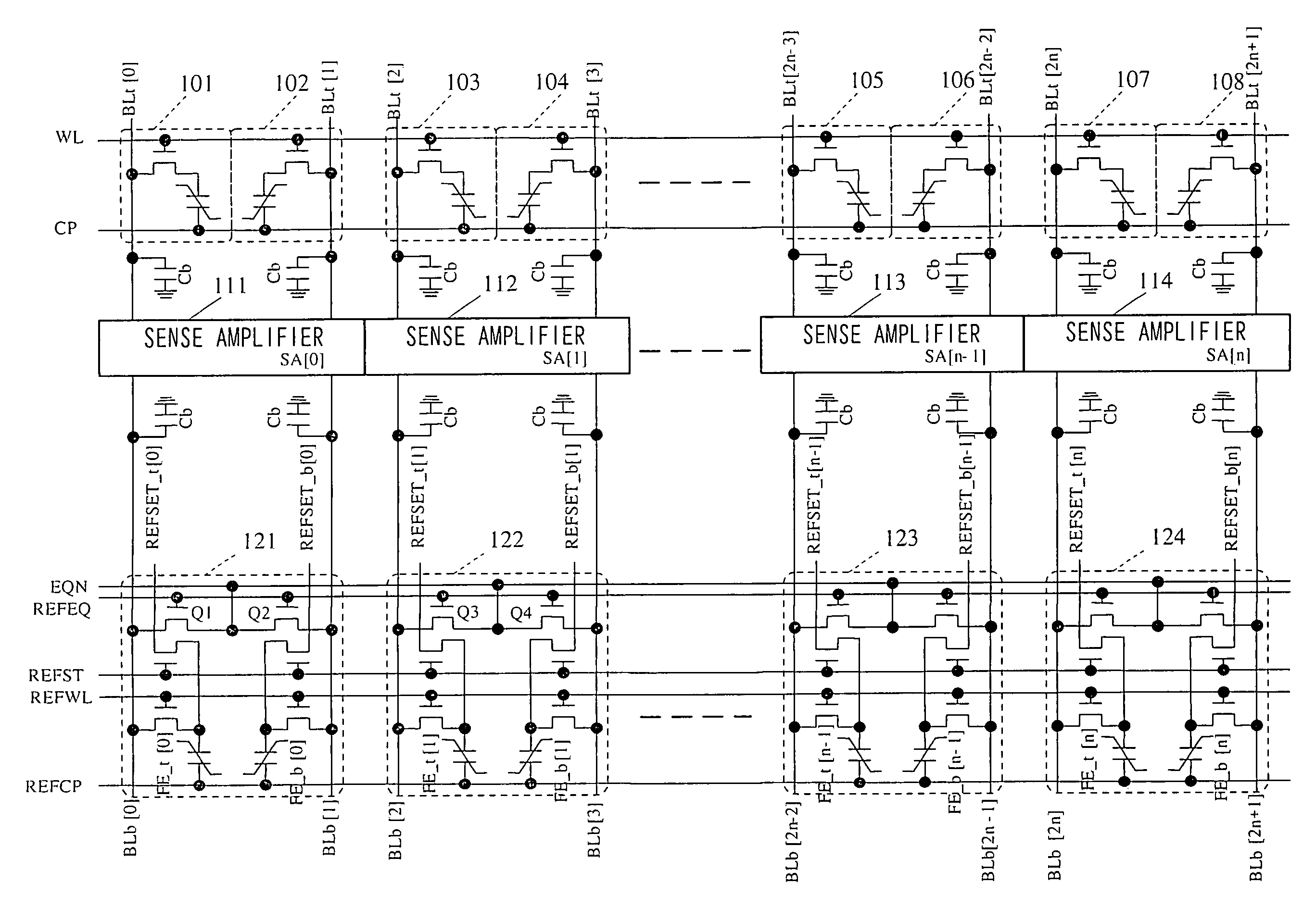
Semiconductor memory device with improved memory retention

a memory device and semiconductor technology, applied in the direction of information storage, static storage, digital storage, etc., can solve the problems of ferroelectric memory having a retention problem, difficult to improve yield, large dispersion of reference potential after retention, etc., and achieve the effect of improving retention problem

Inactive Publication Date: 2006-02-14
PANASONIC CORP
View PDF6 Cites 10 Cited by
  • Summary
  • Abstract
  • Description
  • Claims
  • Application Information

AI Technical Summary

Benefits of technology

[0033]A semiconductor memory device of the present invention comprises a first, second, third and fourth bit lines to be connected to a first, second, third and fourth ferroelectric memory cells respectively, a fifth, sixth, seventh and eighth bit lines to be connected to sense amplifier circuits to be a pair with the first, second, third and fourth bit lines respectively, a first, second, third and fourth reference cell capacitors to be connected to the fifth, sixth, seventh and eighth bit lines respectively when a reference word line is activated, a first, second, third and fourth reference cell write control lines to be connected to the first, second, third and fourth reference cell capacitors when a reference cell write control line select signal is activated, equalization circuits for equalizing the potential of the fifth, sixth, seventh and eighth bit lines when an equalization control signal is activated, and a potential setting circuit for selectively setting an equalization circuit for equalizing the potential of the fifth, sixth, seventh and eighth bit lines when the equalization control signal is activated, and at least one potential of the first, second, third and fourth reference cell write control lines to a first potential or a second potential independently from at least one of the other reference cell write control lines, and by this configuration, desired data can be written to the plurality of reference cell capacitors. And by changing the ratio of the data “0” and the data “1” to be written to the reference cell capacitors, fine adjustment of the reference potential becomes possible, and yield can be improved.
[0036]The semiconductor memory device is also characterized in that the potential setting of the first, second, third and fourth reference cell write control lines by the potential setting circuit is changed depending on the stored data of the non-volatile storage means for each read cycle, so the write data to the reference cells can be changed for each read cycle, and if the write data to the reference cells is changed for each read, imprint can be controlled. The semiconductor memory device has a circuit for detecting the operation environment (e.g. temperature detection), so the reference potential can be adjusted according to the operation environment, and yield can be improved by setting the reference potential to an optimum value.
[0039]The semiconductor memory device is also characterized in that the first terminal of the first reference cell capacitor, the first terminal of the second reference cell capacitor, the first terminal of the third reference cell capacitor and the first terminal of the fourth reference cell capacitor are connected to the first, second, third and fourth reference cell write lines respectively, and a second terminal of the first reference cell capacitor, a second terminal of the second reference cell capacitor, a second terminal of the third reference cell capacitor and a second terminal of the fourth reference cell capacitor are controlled so that the data can be written to the first, second, third and fourth reference cell capacitors, when a memory cell array, including the first, second, third, and fourth ferroelectric memory cells, is not selected, so according to this configuration, retention may become a problem due to the dispersion of the reference potential, but since the write operation of the reference cells can be executed independently, the dispersion of the reference potential can be decreased by writing the reference cells just before reading the memory cells, and the read operation margin increases, and the retention problem can be improved. The write operation of the reference cells can be arbitrarily executed.
[0040]The semiconductor memory device is also characterized in that a power supply detection circuit is included, and the reference cell rewrite operation for rewriting data to the first, second, third and fourth reference cell capacitors after power is applied is automatically executed, so according to this configuration, where the reference cells are automatically written when power is applied, the retention problem can be improved without the user executing the reference cell write operation.

Problems solved by technology

With this, fine adjustment of the reference potential, which is most important in 1T1C operation, cannot be performed, and improving yield is difficult.
Also the dispersion of reference potential after retention is large, so the ferroelectric memory has a retention problem.

Method used


Image

  • Semiconductor memory device with improved memory retention
  • Semiconductor memory device with improved memory retention
  • Semiconductor memory device with improved memory retention

Examples


Embodiment Construction

[0053]Embodiments of the present invention will now be described with reference to FIG. 1 to FIG. 10.

[0054]FIG. 1 shows a configuration of a 1T1C type ferroelectric memory device according to an embodiment of the present invention.

[0055]101 to 108 are 1T1C type ferroelectric memory cells.

[0056]111 to 114 are sense amplifiers for amplifying the potential difference between the bit lines BLt [2n+1:0] and BLb [2n+1:0].

[0057]121 to 124 are reference cells for outputting the reference potential to the bit line BLb [2n+1:0]. FE_t [n:0] and FE_b [n:0] are ferroelectric capacitors. Cb are the parasitic capacitors of the bit lines BLt [2n+1:0] and BLb [2n+1:0].

[0058]WL is a word line to which a select signal for connecting the first terminals of the ferroelectric capacitors of the 1T1C type memory cells 101 to 108 to the bit line BLt [2n+1:0] is applied.

[0059]CP is a cell plate line for driving the second terminals of the ferroelectric capacitors 101 to 108 of the 1T1C type memory cells 101 ...


PUM


Abstract

A semiconductor memory device permitting the data “0” and the data “1” to be arbitrarily written to a reference cell capacitor for generating a reference potential, having a non-volatile capacitor for storing the data to be written. Fine adjustment of the reference potential is possible without a mask correction, which improves yield. The present invention also permits rewriting only the reference capacitors. As such, the dispersion of the reference potential can be controlled, and yield is improved.

Description

BACKGROUND OF THE INVENTION[0001]1. Field of the Invention[0002]The present invention relates to a non-volatile memory device, and more particularly to a reference potential generation technology in the read operation of a 1T1C type ferroelectric memory FeRAM (Ferroelectric Random Access Memory).[0003]2. Description of the Related Art[0004]FIG. 11 shows the configuration of a conventional 1T1C (one transistor one capacitor) type ferroelectric memory. This shows a memory cell array with a 1 row, 2 n column, 1 I / O configuration, where n can be an arbitrary integer.[0005]1001 to 1008 are 1T1C type ferroelectric memory cells. 1011 to 1014 are sense amplifiers for amplifying the potential difference of the bit lines BLt [2n+1:0] and BLb [2n+1:0] which are in a complementary relationship. Cb is a parasitic capacitance of the bit line. 1021 to 1024 are reference cells for generating reference potential. 1031 is a reference potential regulator for adjusting the reference potential.[0006]BLt...

Claims


Application Information

Patent Timeline
Patent Type & Authority Patents(United States)
IPC IPC(8): G11C11/22
CPCG11C11/22
Inventor MURAKUKI, YAUSO
Owner PANASONIC CORP
Why Eureka
Try Eureka