Method for screening failure of memory cell transistor

a cell transistor and gate residue technology, applied in the field of sensing margin measurement of sense amplifiers, can solve the problems of failure of cell transistor trb>13/b>, the failure of the cell transistor trb>13/b> cannot be normally screened, and the gate residue is difficult to normally screen

Active Publication Date: 2006-02-14
INTELLECTUAL DISCOVERY CO LTD
View PDF2 Cites 3 Cited by
  • Summary
  • Abstract
  • Description
  • Claims
  • Application Information

AI Technical Summary

Benefits of technology

[0013]Accordingly, the present invention has been made in an effort to solve the problems occurring in the related art, and an object of the present invention is to provide a method for precisely screening failure of a cell transistor by turning off isolated transistors in a test mode for sensing margin control.

Problems solved by technology

However, when the transistor having the low threshold voltage is used, if a test mode for sensing margin control tm_smc which is a test mode for screening a gate residue of the transistor during the manufacturing process is executed, a breakdown is generated in the transistors composing the sense amplifier before the gate residue is screened.
It is thus difficult to normally screen the gate residue.
In this case, failure of the cell transistor TR13 cannot be normally screened.

Method used


Image

  • Method for screening failure of memory cell transistor
  • Method for screening failure of memory cell transistor
  • Method for screening failure of memory cell transistor

Examples


Embodiment Construction

[0019]Reference will now be made in greater detail to a preferred embodiment of the invention, an example of which is illustrated in the accompanying drawings. Wherever possible, the same reference numerals will be used throughout the drawings and the description to refer to the same or like parts.

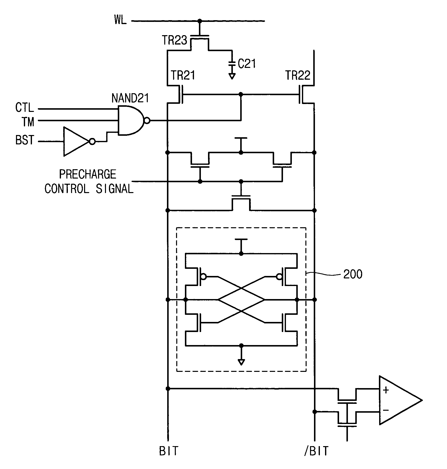
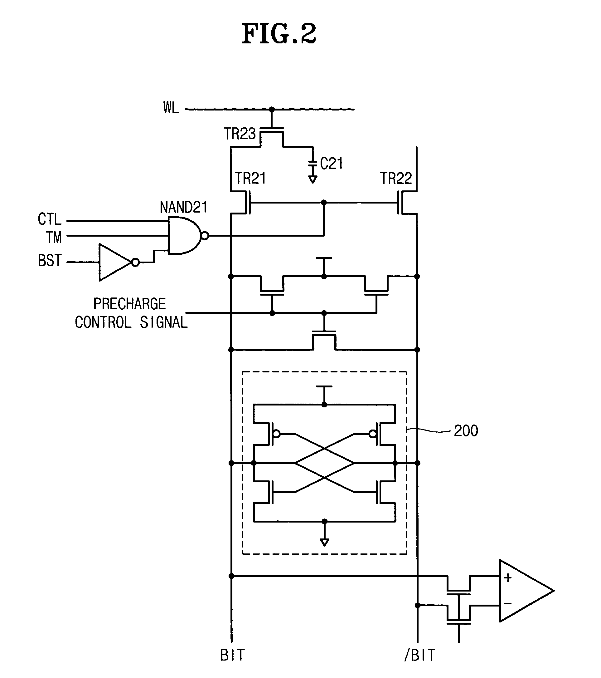
[0020]FIG. 2 is a circuit diagram illustrating peripheral circuits of a memory cell transistor for explaining a method for screening failure of the memory cell transistor in accordance with the present invention.

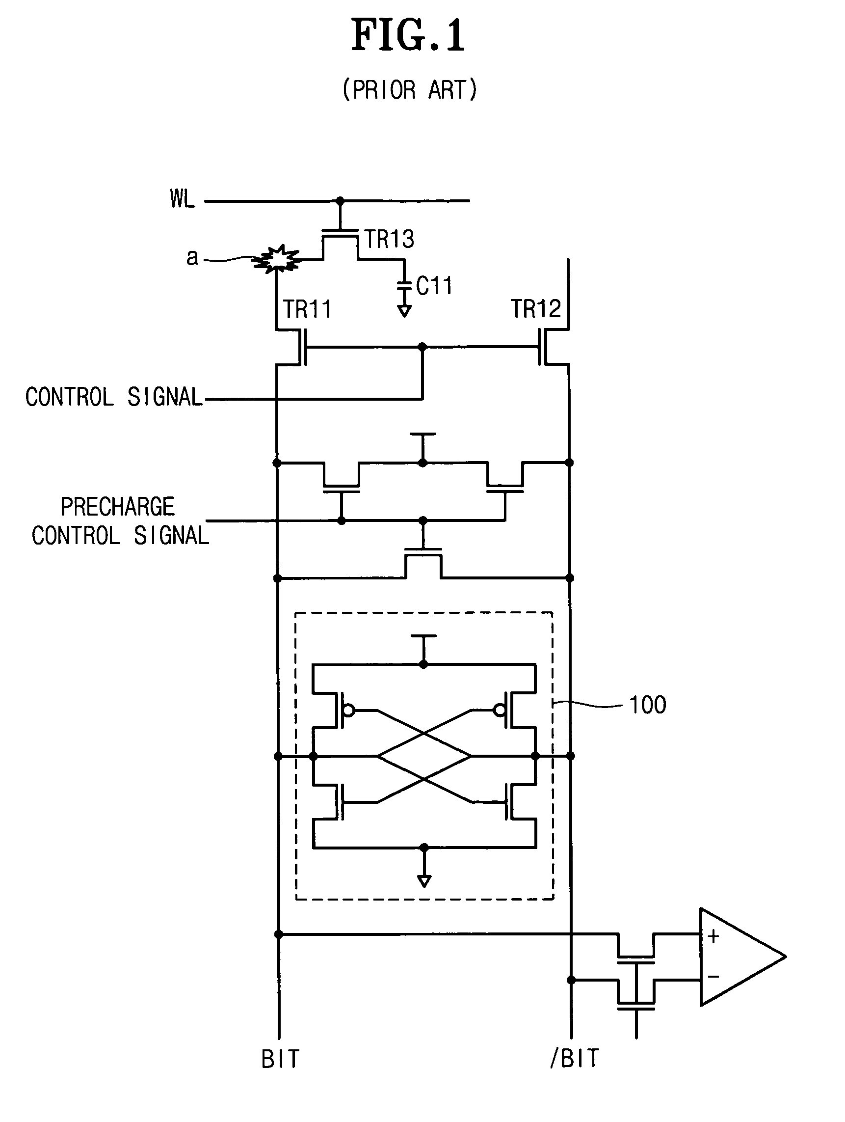
[0021]The circuit of FIG. 2 is identical to the circuit of FIG. 1 except for a NAND gate NAND21 which is a control means for controlling the operation of isolated transistors TR21 and TR22.

[0022]As illustrated in FIG. 2, TM supplied to the NAND gate NAND21 denotes a test mode signal for sensing margin control tm_smc, CTR denotes a control signal enabled by an active command, and BST denotes a burst stop signal. The BST signal ends a burst operation in a normal mode, and enables a s...


PUM


Abstract

The present invention discloses a method for screening a sensing margin generated by a gate residue in a memory cell transistor. The method for screening failure of the memory cell transistor is summarized as follows. A test mode signal for sensing margin control is supplied. A write operation is performed to store data in the cell transistor. A word line is enabled by an active command. Isolated transistors disposed between a bit line coupled to the cell transistor and a bit line coupled to a sense amplifier are disabled to intercept a sensing operation. A voltage of the bit line coupled to the cell transistor is measured for a predetermined time. Here, voltage variations on the bit line are measured to screen failure of the cell transistor.

Description

BACKGROUND OF THE INVENTION[0001]1. Field of the Invention[0002]The present invention relates to a method for measuring a sensing margin of a sense amplifier for a memory device, and more particularly to, a method for measuring a sensing margin generated by a gate residue in a memory cell transistor.[0003]2. Description of the Related Art[0004]In general, high speed memory devices including DDR, DDR2 and DDR3 SDRAM use a transistor having a low threshold voltage to satisfy speed-related specifications such as tRCD, tRP and tAA.[0005]Especially, the transistor having the low threshold voltage is employed for a sense amplifier directly relating to a read operation and peripheral transistors.[0006]However, when the transistor having the low threshold voltage is used, if a test mode for sensing margin control tm_smc which is a test mode for screening a gate residue of the transistor during the manufacturing process is executed, a breakdown is generated in the transistors composing the s...

Claims


Application Information

Patent Timeline
Patent Type & Authority Patents(United States)
IPC IPC(8): G11C29/00G11C7/06G11C11/34
CPCG11C29/50G11C11/40A23B7/02F26B3/02F26B21/08F26B25/005F26B25/04
Inventor KIM, YOUNG SOOLEE, JUNG HOON
Owner INTELLECTUAL DISCOVERY CO LTD
Why Eureka
Try Eureka