Sample preparation for transmission electron microscopy

a transmission electron microscopy and sample technology, applied in the field of sample preparation for transmission electron microscopy, can solve the problems of significantly greater margin amorphization, insufficient thinness of lamella, and inability to yield the desired sample quality, and achieve the effect of high degree of detail

Active Publication Date: 2006-02-21
LEICA MICROSYSTEMS GMBH
View PDF3 Cites 67 Cited by
  • Summary
  • Abstract
  • Description
  • Claims
  • Application Information

AI Technical Summary

Benefits of technology

[0008]The formation according to the invention of a sample, in particular of a sample lamella, permits the production of a sufficiently thin lamella, which during the TEM observation can resolve and image a high degree of detail of the original sample material. For this purpose according to the invention a coarse sample produced with the FIB technique is subsequently worked with an ion beam and thinned or etched to the requisite thickness. The subsequent working of the sample must be free of contamination, which means no foreign material, such as ambient material or none of the original material must again be deposited onto the sample during the etching process. A further important aspect comprises that in this subsequent working the material structure of the sample is not altered on the surface, or that the original structure of the sample material is retained. Since the FIB sample as the starting sample already has structural disturbances, such as margin amorphization, on the surfaces, which are inherent to the FIB technique, and extend approximately to a depth of 20 nm into each sample side, it is necessary that the subsequent working technique can to a substantial extent eliminate such areas of disturbance in order to expose the original not affected material which is to be analyzed. According to the invention this is attained thereby that the sample is bombarded and ablated alternately on both sides by an ion beam at a bombardment angle. It becomes thereby possible to avoid to a large extent contaminations, which is absolutely necessary for high-resolution transmission electron microscopy (HRTEM). The method according to the invention now also permits producing the appropriately thin samples of less than 40 nm thickness, even preferably of less than 20 nm thickness, which are required for this high-resolution technology. A further advantage comprises that the subsequent working according to the invention is applicable to all FIB sample types and does not depend on the sample geometry. Complicated sample geometries can thus also be worked subsequently.
[0009]In order to avoid preferential directions of the ion beam etching, thus undesired scoring structures on the sample surface, it is advantageous to move, in addition, the sample relative to the ion beam. Such movements can be oscillating movements and be carried out as periodic tilting movements of the sample relative to the direction of incidence of the ion beam. This movement should be relatively slow and uniform. The tilting can advantageously take place by an angle of up to ±70 degrees relative to the ion beam direction and the movement frequency approximately in a range of 0.1 Hz.

Problems solved by technology

However, this does not yield the desired quality of the sample appropriate to current requirements.
The wet-chemical etching method does not lead to the desired goal.
The lamella cannot be prepared of sufficient thinness for the samples to be well suited for high-resolution transmission electron microscopy (HRTEM).
The TEM lamella is moreover contaminated through the preparation and, in comparison to conventional ion beam preparation with fixed ion beam, has significantly greater margin amorphization.
However, the advantages, such as for example the target precision of the scanning FIB technique cannot be attained.
The above listed problems lead to a strongly reduced sample quality.
But, due to the sample geometry and the etching on one side of the lamella, additional undesirable contamination occurs.
Such contaminations negate the advantage of the subsequent treatment and make the sample unusable.

Method used


Image

  • Sample preparation for transmission electron microscopy
  • Sample preparation for transmission electron microscopy
  • Sample preparation for transmission electron microscopy

Examples


Embodiment Construction

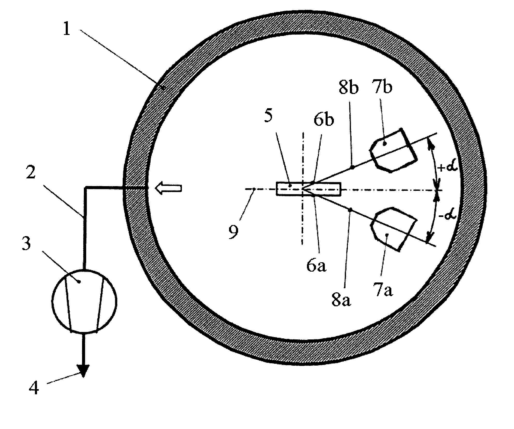
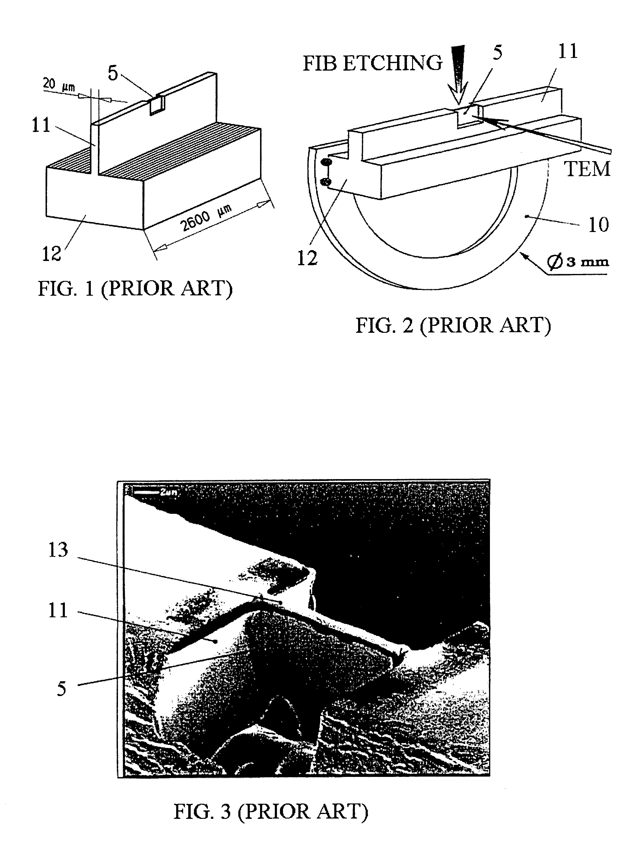
[0016]For the production of an FIB sample from the solid body material, for example from a semiconductor wafer, a sample piece 12 is removed and on it through mechanical sawing a web 11 is roughed out, such as is shown for example in FIG. 1. The sample piece 12 is approximately 2600 μm long and the width of the web is approximately 20 μm. On the front face of the web 11 in a partial region where the lamella sample 5 is to be generated, a protective coating is applied which serves as masking for the subjacent lamella 5 which is to be etched out. With a focused ion beam (FIB) impinging perpendicularly on the front face of the web the lamella 5 is now exposed by depth etching. This is schematically shown in FIG. 2 by the arrow with the label “FIB etching”.

[0017]The sample piece 12 with the lamella sample 5 is now disposed on a sample holder 10 with a diameter of for example 3 mm, and can now be observed in the TEM, as is also indicated schematically in FIG. 2 by the arrow and the assoc...


PUM

PropertyMeasurementUnit
thicknessaaaaaaaaaa
thicknessaaaaaaaaaa
disturbance depthaaaaaaaaaa

Abstract

TEM FIB samples of a solid state material are subsequently thinned through a subsequent treatment step free of contamination and free of destruction to extremely thin thicknesses through the alternate-sided bombardment of the sample surfaces with an ion beam, with which high-resolution observation and analysis of the sample material with a TEM becomes possible.

Description

FIELD AND BACKGROUND OF THE INVENTION[0001]The invention relates to a TEM FIB sample as well as to a method for the production of such a sample.[0002]Samples for transmission electron microscopy (TEM) can be prepared in different ways. To be able to observe samples with a TEM, these must be thinned correspondingly defined such that they can be transmitted by electrons in the TEM. The quality of the image resolution is substantially dependent on the quality of the sample. For this purpose the sample must be uniformly set to a correspondingly desired defined thickness in a corresponding etching process. It is here important that in this etching process the sample structure is not altered by the process itself. However, this does not yield the desired quality of the sample appropriate to current requirements. The wet-chemical etching method does not lead to the desired goal.[0003]For this reason, for high-quality TEM samples the samples are today worked by etching with a fixed argon io...

Claims


Application Information

Patent Timeline
Patent Type & Authority Patents(United States)
IPC IPC(8): G01N1/28G01N1/04G01N1/32H01J37/305
CPCG01N1/32H01J37/3056H01J2237/31745
Inventor GRUNEWALD, WOLFGANG
Owner LEICA MICROSYSTEMS GMBH
Why Eureka
Try Eureka