Method for printing an image on a printing substrate and device for inputting energy to a printing-ink carrier

Inactive Publication Date: 2006-02-21
HEIDELBERGER DRUCKMASHINEN AG
22 Cites 43 Cited by

AI-Extracted Technical Summary

Problems solved by technology

A clear disadvantage of scanning is the fact that only a limited maximum speed is achievable.
An exact synchronization of the movements of the deflecting mirror and of the paper transport at extremely different speeds can only be achieved with great effort; for example, it is required to use piezoelectric mirrors.
As a rule, a large installation space is needed.
The risk of damage to optical components increases, but also the possibility of an unwanted modification of involved materials, such as the printing ink itself.
Through the use of a plurality of laser light sources, such as a line of laser light sources, the requirements in terms of power, modulation frequency, and scanning speed are, in fact, reduced, but the coupling-in of two light beams into a polygon scanner is technically already very difficult to implement.
For example, fifty light beams, each modulated at 4 MHz, are to be considered extremely difficult.
Page-wide arrays or arrangements of light-emitting diodes (LED), as are widespread, for example, in electrophotographic printing presses,...

Method used

[0051]In the embodiment with bottom emitters, the emitters are contacted via conductor tracks that are provided in an electrically insulating substrate, such as a diamond substrate. In the case of bottom emitters, it is advantageously avoided that a number of bonding wires are arranged on the light exit side which could possibly hinder the exit of light. If the n-doped side of the light source is up and the p-doped side of the light source is down, then the substrate surface opposite the p-doped side must be patterned. The substrate itself is attached to a heat sink, preferably to a patterned heat sink, such as a microchannel cooler, so that adequate and efficient heat transfer is provided between the substrate and the heat sink. In this embodiment, the current sources for the VCSEL light sources are situated in the immediate vicinity of the light sources on one...

Benefits of technology

[0014]Considering the disadvantages of the prior art, it is an object of the present invention to provide a method for printing an image on a printing substrate, including a powerful energy source, and a device for inputting energy to a printing-ink carrier. In particular, a device for inputting energy is intended to be equi...

Abstract

A method for printing an image on a printing substrate, a number of portions of fluid printing ink being produced on a printing ink carrier (10) through energy input by a number of image spots (810) of an array (84) of individually controllable VCSEL light sources, and the fluid printing ink being transferred to the printing substrate. A device for inputting energy (80) to a printing-ink carrier (10), includes a number (82) of individually controllable laser light sources which have a modular design consisting of subarrays (86) and are disposed in an array (84), and further includes printing-ink carrier (10) with which is associated an axis of rotation (88) and on the surface of which can be produced a number of image spots (810) of the laser light sources. The subarrays of laser light sources are VCSEL bars (84), and rows of image spots (12) of the VCSEL bars are inclined with respect to the axis of rotation (88).

Application Domain

Printing platesOther printing apparatus +2

Technology Topic

Image

  • Method for printing an image on a printing substrate and device for inputting energy to a printing-ink carrier
  • Method for printing an image on a printing substrate and device for inputting energy to a printing-ink carrier
  • Method for printing an image on a printing substrate and device for inputting energy to a printing-ink carrier

Examples

  • Experimental program(1)

Example

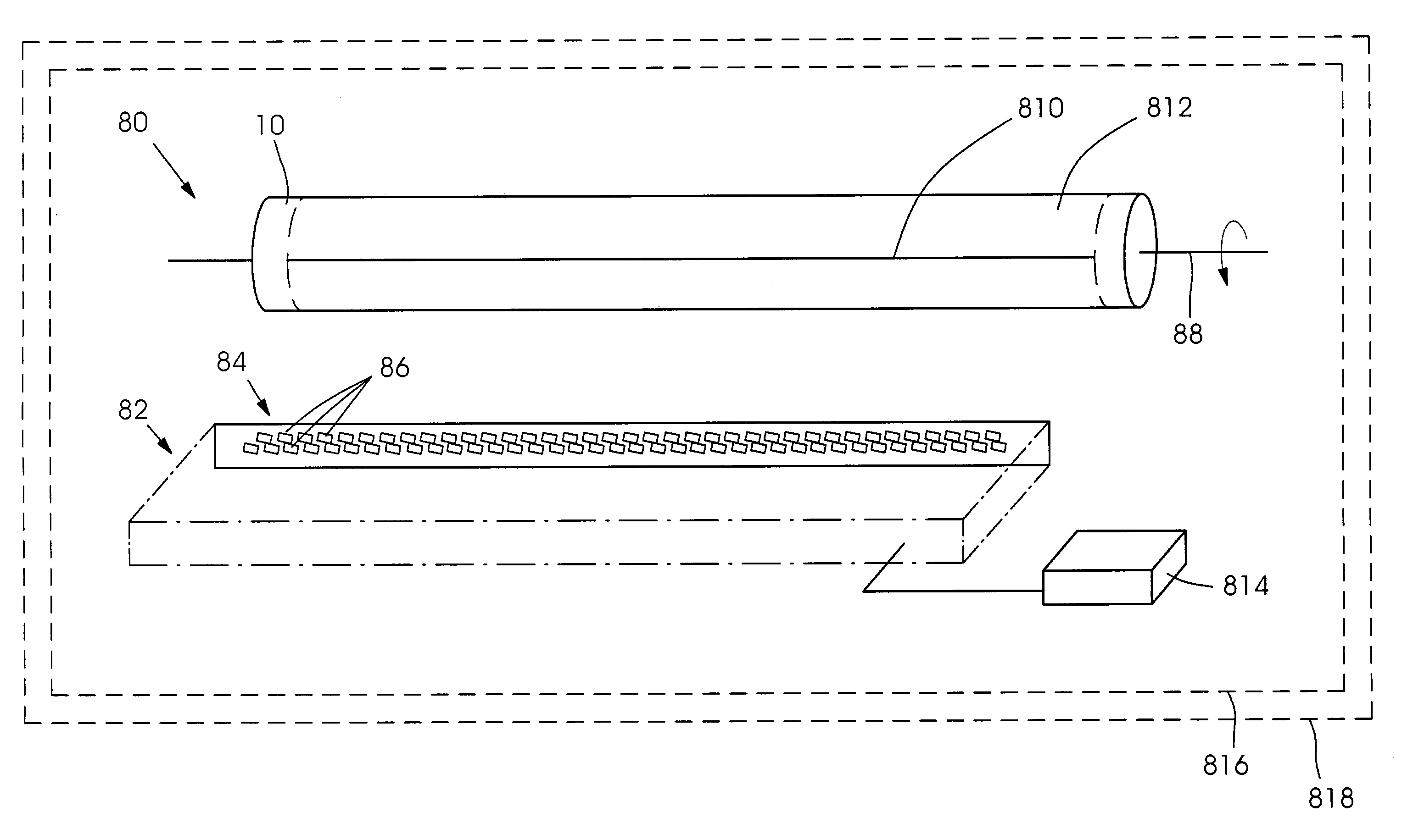
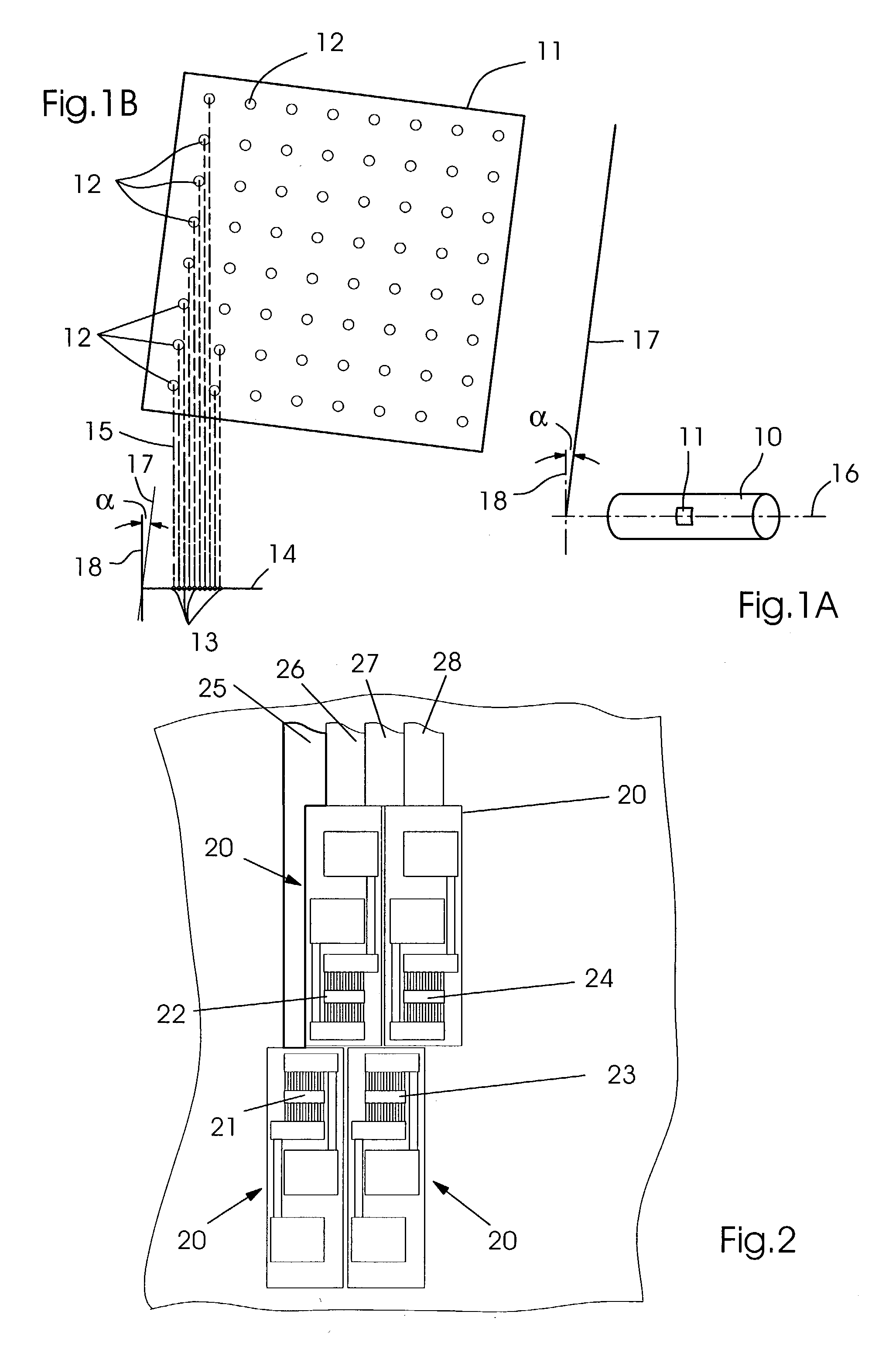
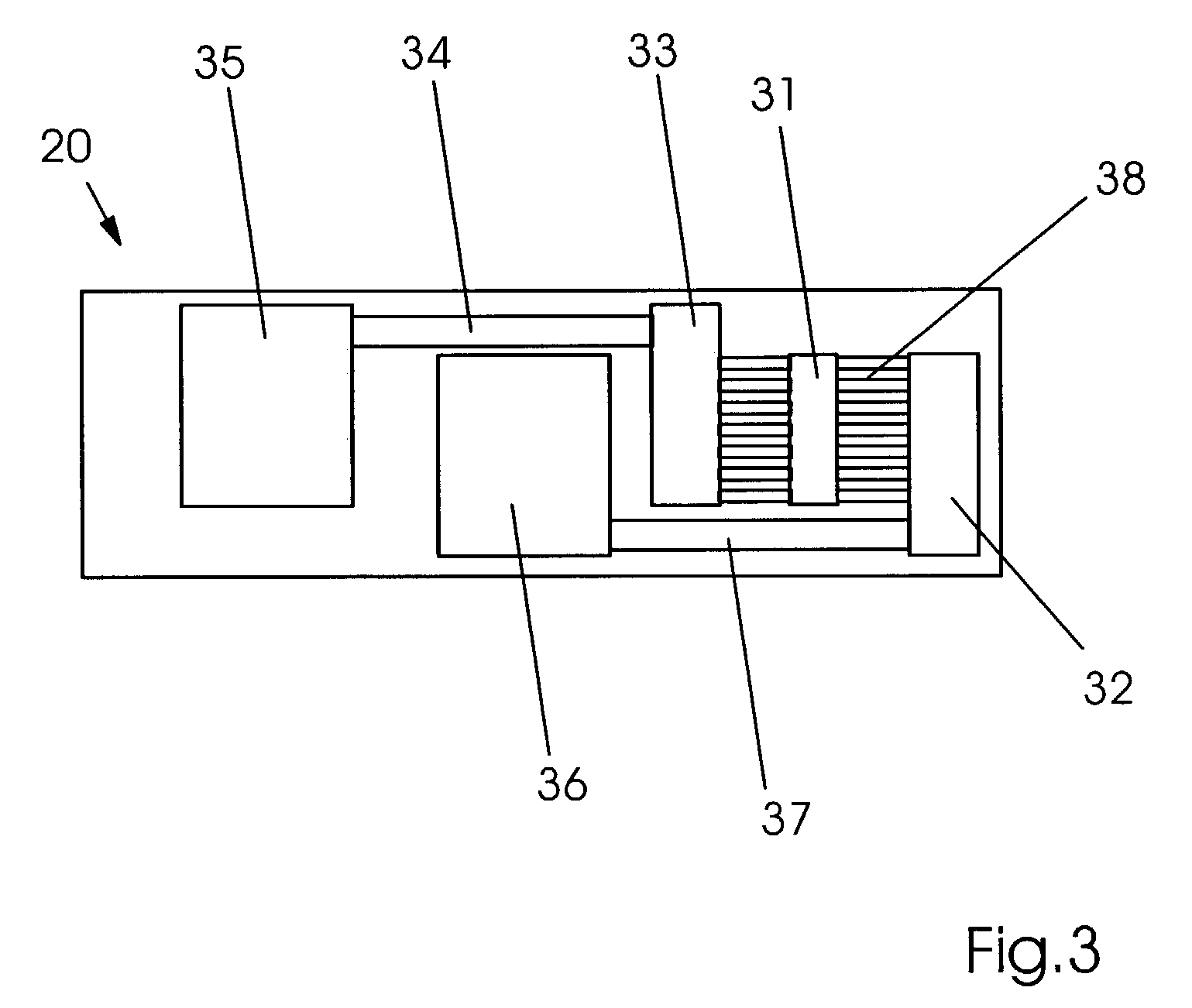
[0048]In FIG. 1, the relative position of the number of image spots 12 on a printing-ink carrier 10 in the inventive device for inputting energy to a printing-ink carrier 10 is shown in Subfigures 1A and 1B) for the purpose of illustration. Subfigure 1A of FIG. 1 depicts an advantageous embodiment of a printing-ink carrier 10. Printing-ink carrier 10 is a cylinder body, represents the lateral surface of a cylinder partially or in its entirety, or is held on a cylinder. Printing-ink carrier 10 is designed such that it can rotate about an axis of rotation 16. Segment 11 of the surface of printing-ink carrier 10 is the region where image spots of a VCSEL bar come to rest when triggered simultaneously. The image spots are regularly arranged on intersection points of a Cartesian grid. The axes defining the grid are rotated by inclination angle α with respect to axis of rotation 16 and to the normal (perpendicular) 18 to the axis of rotation: unfolding direction 17 and normal 18 form inclination angle α.
[0049]Subfigure 1B of FIG. 1 shows an enlarged detail of Subfigure 1A. Subfigure 1B shows segment 11 of the surface of printing-ink carrier 10 including a number of image spots 12 in a regular and Cartesian arrangement for the case that the VCSEL light sources are triggered or tripped simultaneously. Rows of image spots 12 located along an unfolding direction 17 are projected onto a line 14 by delayed or advanced triggering or tripping of the VCSEL light sources if the imaging beams producing the image spots, in particular, the light sources, and the surface of the printing-ink carrier move relative to each other. If line 14 is parallel to axis of rotation 16 and forms an inclination angle α with an unfolding line of the Cartesian grid of n×m image spots 12 (n image spots along unfolding line 17), the projected spots 13 of image spots 12 are dense, that is, they have the minimum printing dot spacing, if the condition tan α=1/n is fulfilled.
[0050]FIG. 2 shows an advantageous embodiment of the arrangement of imaging modules 20 in the device according to the present invention for inputting energy to a printing-ink carrier. An array of VCSEL light sources can be made up of such imaging modules 20. In the embodiment shown in FIG. 2, an imaging module carries a VCSEL bar which, by way of example, has 256 VCSEL light sources or emitters. The geometry of the emitters in the VCSEL bar is, by way of example, 32×8 emitters, in a regular and Cartesian arrangement, that is, in a rectangular raster or on a rectangular grid, with a spacing of 320 micrometers between the centers of neighboring light sources. For a format size of 34 centimeters and an image spot size of 40 micrometers, 34 VCSEL bars each with 256 VCSEL light sources are required. Preferred are numbers of light sources on a VCSEL bar that are powers of 2. The imaging modules, that is, the VCSEL bars or subarrays, are arranged inclined with respect to the axis of rotation of a cylindrical printing-ink carrier in such a manner that the projected spots of the image spots of the emitters are evenly spaced on the lateral surface of the printing-ink carrier (in this respect, see also FIG. 1).
[0051]In the embodiment with bottom emitters, the emitters are contacted via conductor tracks that are provided in an electrically insulating substrate, such as a diamond substrate. In the case of bottom emitters, it is advantageously avoided that a number of bonding wires are arranged on the light exit side which could possibly hinder the exit of light. If the n-doped side of the light source is up and the p-doped side of the light source is down, then the substrate surface opposite the p-doped side must be patterned. The substrate itself is attached to a heat sink, preferably to a patterned heat sink, such as a microchannel cooler, so that adequate and efficient heat transfer is provided between the substrate and the heat sink. In this embodiment, the current sources for the VCSEL light sources are situated in the immediate vicinity of the light sources on one or more semiconductor components which can be attached to or accommodated on the same substrate as the VCSELs, or which can be attached to or accommodated on a separate substrate on the same or a different heat sink.
[0052]The beam shaping of the laser light emerging from the emitters can be accomplished using micro-optical components (acting on only one or more light beams of the VCSEL bar) and/or macro-optical components (acting on all light beams of the VCSEL bar). Suitable for beamshaping are, in particular, arrays of micro-optical components, such as microlens arrays, where the spacing between the individual components corresponds to the spacing of two laser emitters or a multiple thereof.
[0053]Since two neighboring imaging modules 20 or neighboring VCSEL bars cannot be placed close enough to write neighboring lines densely (at 600 dpi 40 micrometers), the two-row arrangement shown in FIG. 2 is particularly advantageous. Preferred is an arrangement in two rows, where the distance of the VCSEL bars of two neighboring imaging modules 20 in the circumferential direction of the cylindrical printing-ink carrier is as small as possible. Imaging modules 20 which are shown in FIG. 2 and include first VCSEL bar 21, second VCSEL bar 22, third VCSEL bar 23, and fourth VCSEL bar 24 image strips which are located on printing-ink carrier 10 densely side-by-side: first strip 25 is imaged by first VCSEL bar 21, second strip 26 by second VCSEL bar 22, third strip 27 by third VCSEL bar 23, and fourth strip 28 is imaged by fourth VCSEL bar 24.
[0054]FIG. 3 schematically relates to an advantageous embodiment of imaging modules 20 in the device according to the present invention. A difficulty in supplying power to a two-dimensional arrangement of VCSEL light sources on one bar is to lead through the conductor tracks narrowly enough between the emitters of the rows at the edge. Here, it is advantageous for the feed lines for one half of the emitters to come from one direction and for the other half of the emitters to come from the other direction. FIG. 3 serves to illustrate this advantageous geometry or configuration in greater detail. FIG. 3 shows the design of one embodiment of an imaging module 20 having a VCSEL bar 31. VCSEL bar 31 is connected to first drive electronics 32 (driver chip) for a first half of the number of VCSEL light sources on the bar and second drive electronics 33 (driver chip) for a second half of the number of VCSEL light sources on the bar. First drive electronics 32 is interactively connected to a first electronics boards 36 via a first connecting line 37. Second drive electronics 33 is interactively connected to a second electronics boards 35 via a second connecting line 34. First and second electronics boards 35, 36 are provided with the required terminals, power supply, and clock generation for driving the light sources. First and second drive electronics 32, 33 are connected to the VCSEL light sources on VCSEL bar 31 via parallel conductor tracks 38. Conductor tracks 38 contact the VCSEL bar from two sides.
[0055]FIG. 4 is a schematic diagram to illustrate an embodiment of the method according to the present invention for printing an image on a printing substrate, the number of portions of fluid printing ink being produced by melting solid printing ink, which is located on the printing-ink carrier and exhibits delayed solidification, on a dot-by-dot or pixel-by-pixel basis. Shown is a section perpendicular to the direction of rotation of a printing-ink carrier. Printing-ink carrier 10 has a layer of solid printing ink 40, preferably homogenous and smooth. The printing ink is capable of being melted, softened or liquefied and solidifies in a delayed manner or with a delay (temperature hysteresis of the phase transition or temperature hysteresis of viscosity). A light source 42 of a row of VCSEL bars (not shown in this diagram) essentially parallel to the axis of rotation of printing-ink carrier 10 selectively and controllably emits laser light 44 which impinges on solid printing-ink 40. The light sources are located outside printing-ink carrier 10. Melted portions 46 of fluid printing ink are selectively and controllably produced by the thermal action of laser light 44. A pattern is produced. Due to the temperature hysteresis of the phase transition, melted portions 46 still remain liquid while the fluid printing ink already cools on the way to printing nip 414. In printing nip 414, a printing substrate 410 is pressed against the printing ink through interaction of printing-ink carrier 10 with an impression cylinder 412. In printing nip 414, portions 46 of fluid printing ink can be partially or completely transferred to printing substrate 410. Provision is made for a regeneration device 416 which makes it possible to restore a homogeneous layer of solid printing ink 40. The quantity of transferred ink lost at spots that were melted is compensated for and the surface is smoothed. In this manner, a cyclic process of imaging and regeneration is created, since solid printing ink 40 can be imaged again. The described printing method is variable and digital.
[0056]Alternatively to the situation shown in FIG. 4, the light sources can also be located inside printing-ink carrier 10. If the selective and controlled melting takes place in the immediate vicinity of printing nip 414 prior to contact with printing substrate 410, the described method can also be carried out using printing ink without solidification delay.
[0057]FIG. 5 is a schematic diagram to illustrate an embodiment of the method according to the present invention for printing an image on a printing substrate, the number of portions being produced by suctioning fluid printing ink into depressions on a dot-by-dot or pixel-by-pixel basis upon cooling of the volumes of the depressions that were heated by the energy input (suction pressure method). Shown is a section perpendicular to the direction of rotation of a printing-ink carrier. Printing-ink carrier 10 has a surface 50 with despressions 52. Depressions 52 form a regular, fine raster of volumes in the surface. A light source 54 of a row of VCSEL bars (not shown in this diagram) essentially parallel to the axis of rotation of the printing-ink carrier selectively and controllably emits laser light 56 which hits the volumes of the depressions 52. During the rotation of printing-ink carrier 10, surface 50 with depressions 52 passes a reservoir 58 containing fluid printing ink 510. Alternatively to the situation shown in FIG. 5, laser light source 54 or, to be more precise, the VCSEL bars can also be located inside printing-ink carrier 10. Laser light 56 is preferably radiated into the volumes of depressions 52 shortly before these volumes plunge into reservoir 58. Through the selective and controlled action of laser light 56, the air is heated differently in different depressions 52, thus producing different air displacements. When the air in the volumes of depressions 52 cools, fluid printing ink is suctioned into depressions 52 selectively and in controlled quantities. Provision is made for a stripping means (a doctor blade, a wiper, or the like) which removes excess printing ink from the raised portions of surface 50. The depressions 512 filled with printing ink reach printing nip 518 through the rotation of printing-ink carrier 10. A printing substrate 516 is pressed against surface 50 with depressions 52, in particular, with depressions 512, through interaction of printing-ink carrier 10 with an impression cylinder 520, allowing printing ink to be transferred to printing substrate 516. Transferred printing ink 514 solidifies on printing substrate 516. During the transfer of printing ink, the depressions 512 filled with printing ink are partially or completely emptied. Finally, provision is made for a cleaning device 522, which is used to prepare surface 50 for a new sequence of the steps of the printing method. The depressions 52 of surface 50 are cleaned from ink residues, so that surface 50 is reset to the starting condition for the method. Thus, the described printing method is a variable or digital method.
[0058]FIG. 6 shows a schematic diagram to illustrate an embodiment of the method according to the present invention for printing an image on a printing substrate, the number of portions of fluid printing ink being produced by detachment from a printing-ink layer 60. Shown is a section perpendicular to the direction of rotation of a printing-ink carrier. Printing-ink carrier 10 has a printing-ink layer 60 on its surface. Printing-ink layer 60 can be solid or liquid (preferred). Located inside printing-ink carrier 10, which rotates about its axis, is a laser light source 62 of a row of VCSEL bars (not shown in this diagram) which are arranged essentially parallel to the axis of rotation of the printing-ink carrier. Laser light source 62 selectively and controllably emits laser light 64. Laser light 64 impinges on printing-ink layer 60 in a region where printing-ink layer 60 is homogeneous and unpatterned. Via the light-hydraulic effect, the energy of the laser light allows detachment of portions of fluid printing ink 66, directly (in printing-ink layer 60 ) or indirectly (by conversion into acoustic energy, through production of thermal energy and the accompanying volume change in printing-ink carrier 10). A portion of fluid printing ink 66 also has an impulse, so that the portion is thrown against the surface of a printing substrate 68. Using a regeneration device 610, the surface of printing-ink layer 60 can be prepared to be used again by restoring a homogeneous and unpatterned surface. The detached quantity of ink can be replaced by applying further printing ink, during which the surface can be smoothed at the same time. Thus, the described printing method is a variable or digital method, since the restored starting condition allows the printing process to be carried out again.
[0059]FIG. 7 is a schematic diagram to illustrate an embodiment of the method according to the present invention for printing an image on a printing substrate 712, the number of portions of fluid printing ink being produced by expelling from depressions 72 in a surface 70 of a printing-ink carrier 10. Shown is a section perpendicular to the direction of rotation of printing-ink carrier 10. Printing-ink carrier 10 has a surface 70 with depressions 72, in particular depressions 74 that are filled with printing ink, and is rotatable about its axis. Located inside printing-ink carrier 10 is a laser light source 76 of a row of VCSEL bars (not shown in this diagram) which are arranged essentially parallel to the axis of rotation of the printing-ink carrier. Laser light source 76 selectively and controllably emits laser light 78. Laser light 78 impinges on surface 70 with depressions in a region where the depressions are homogeneously filled with printing ink. Energy input into a depression 74 filled with printing ink occurs such that the printing ink is pressed out, expelled or thrown out from depression 74, while printing substrate 712 contacts or touches surface 70 of printing-ink carrier 10 or is pressed against the surface. The depressions 74 filled with printing ink are partially or completely emptied in a selective and controlled manner by transferring the printing ink to printing substrate 712. As the rotation continues, depressions 72 pass a regeneration device 714. Depressions 72 are homogeneously filled with printing ink again, allowing the described printing method to be carried out repeatedly. The printing method is variable or digital.
[0060]FIG. 8 shows an embodiment of a device 80 according to the present invention in a printing unit 816 of a printing press 818, where printing-ink carrier 10 is a cylinder, or the surface of a cylinder, or is held on a cylinder. In this embodiment, a page-wide array 84 of VCSEL light sources made up of VCSEL bars 86 in a two-dimensional arrangement of the channels or imaging beams is used for a variable printing method, such as described with reference to FIGS. 4, 5, 6 and 7. The variable printing method is preferably a digital printing process in which meltable printing ink is liquefied or softened on the printing-ink carrier using laser radiation, allowing the fluid printing ink to be transferred to the printing substrate in the liquid state (in this respect, see also FIG. 4). Each VCSEL light source or each emitter generates sufficient output power, typically 200 mW, in a beam of sufficient optical quality. The VCSEL can be driven individually. The array is made up of small modules or subarrays. The channels are dense, which means that the lines that can be written by the modules during one rotation of the cylinder produce a solid area.
[0061]FIG. 8 shows an embodiment of the device according to the present invention for inputting energy 80, including a number of individually controllable laser light sources 82 in the form of an array 84 of subarrays, the subarrays being or including VCSEL bars 86. A cylindrical printing-ink carrier 10, which is rotatable about an axis of rotation 88, is arranged opposite the individually controllable laser light sources 82. The VCSEL bars are arranged such that they are tilted by an inclination angle with respect to axis of rotation 88. Laser light sources 82 can be controlled selectively and independently of each other, in particluar in terms of optical output power, temporal tripping (power-on and power-off), and duration of the light emission. The laser light sources are connected to a control unit 814. In the case of delayed or advanced triggering, that is, when triggereing laser light sources 82 at varied points in time, the emitted laser light produces on the surface a line 810 of placed image spots according to the procedure already explained in detail with reference to FIG. 1. Array 84 is page-wide. In other words, page-wide surface area 812 of printing-ink carrier 10 is densely illuminated by the image spots of laser light sources 82, so that energy input for the creation of printing dots is possible over the complete page width. Inside printing unit 816 of printing press 818, provision is made for means (not graphically depicted here) for printing or transferring the pattern of the printing-ink carrier produced by input of energy or the portions of fluid printing ink to a printing substrate. The tripping of laser light sources 82 is coordinated with the rotation of printing-ink carrier 10. To this end, the machine control, the drive for the rotation of printing-ink carrier 10, and control unit 814 are in communication to exchange data and/or control signals.
[0062]In this connection, it should also be mentioned that it is possible to carry out an automatic calibration at regular intervals by means of control unit 814 in order to compensate for deviations of the performance curves of the VCSEL light sources on a bar or in an array that are due to ageing. Since deviations of the performance curves of individual emitters of an array rarely occur in VCSEL light sources on one bar or are insignificant, it is even possible to limit such a calibration to one emitter or a small number of emitters a subarray, respectively. The resulting measured current can be used with sufficient accuracy for all light sources.
[0063]FIG. 9 shows an embodiment of a device according to the present invention which is located inside printing-ink carrier 10 and illuminates printing-ink carrier 10 from its underside 90. In this embodiment, a page-wide array 84 of VCSEL light sources made up of VCSEL bar 86 in a two-dimensional arrangement of the channels or imaging beams is used for a variable printing method, such as described with reference to FIGS. 4, 5, 6 and 7. Inside printing unit 816 of printing press 818, provision is made for means (not graphically depicted here) for printing or transferring the pattern of the printing-ink carrier produced by input of energy or the produced portions of fluid printing ink to a printing substrate. Cylindrical printing-ink carrier 10 is rotatable about an axis of rotation 88. The VCSEL bars of light sources 82 are arranged such that they are tilted by an inclination angle with respect to axis of rotation 88 of printing-ink carrier 10 (in this respect, see also FIGS. 1 and 8 ). Laser light sources 82 can be controlled selectively and independently of each other, in particluar in terms of optical output power, temporal tripping (power-on and power-off), and duration of the light emission. The laser light sources are connected to a control unit, which is not graphically depicted here. In the case of delayed or advanced triggering, that is, when tripping laser light sources 82 at varied points in time, the emitted laser light produces on the surface a line 810 of placed image spots according to the procedure already explained in detail with reference to FIG. 1. Printing-ink carrier 10 is designed such that it is transparent to the used wavelength of the laser light of the VCSEL bars so that the printing ink on the surface of printing-ink carrier 10 or the depressions of the surface of printing-ink carrier 10 are reached by the laser light. Array 84 is page-wide. In other words, page-wide surface area 812 of printing-ink carrier 10 is densely illuminated by the image spots of laser light sources 82, so that energy input for the creation of printing dots is possible over the complete page width.
[0064] List of Reference Numerals 10 printing-ink carrier 11 surface segment of the printing-ink carrier 12 image spot 13 projected spot of an image spot 14 line 15 projection 16 axis of rotation 17 unfolding direction α inclination angle 18 normal to the axis of rotation 20 imaging module 21 first VCSEL bar 22 second VCSEL bar 23 third VCSEL bar 24 fourth VCSEL bar 25 first strip imaged by the first VCSEL bar 26 second strip imaged by the second VCSEL bar 27 third strip imaged by the third VCSEL bar 28 fourth strip imaged by the fourth VCSEL bar 31 VCSEL bar 32 first drive electronics 33 second drive electronics 34 second connecting line 35 second electronics board 36 first electronics board 37 first connecting line 38 parallel conductor tracks to VCSELs on the bar 40 solid printing ink 42 laser light source 44 laser light 46 melted portions of fluid printing ink 48 transferred printing ink 410 printing substrate 412 impression cylinder 414 printing nip 416 regeneration device 50 surface with depressions 52 depressions 54 laser light source 56 laser light 58 reservoir 510 fluid printing ink 512 depressions filled with printing ink 514 transferred printing ink 516 printing substrate 518 printing nip 520 impression cylinder 522 cleaning device 60 printing-ink layer 62 laser light source 64 laser light 66 portions of fluid printing ink 68 printing substrate 610 regeneration device 70 surface with depressions 72 depressions 74 depressions filled with printing ink 76 laser light source 78 laser light 710 expelled portions of fluid printing ink 712 printing substrate 714 regeneration device 80 device for inputting energy 82 number of individually controllable laser light sources 84 array of subarrays 86 VCSEL bar 88 axis of rotation 810 line of placed image spots 812 page-wide surface area 814 control unit 816 printing unit 818 printing press 90 underside of the printing-ink carrier

PUM

no PUM

Description & Claims & Application Information

We can also present the details of the Description, Claims and Application information to help users get a comprehensive understanding of the technical details of the patent, such as background art, summary of invention, brief description of drawings, description of embodiments, and other original content. On the other hand, users can also determine the specific scope of protection of the technology through the list of claims; as well as understand the changes in the life cycle of the technology with the presentation of the patent timeline. Login to view more.

Similar technology patents

Combined gain-soa chip

Owner:FRAUNHOFER GESELLSCHAFT ZUR FOERDERUNG DER ANGEWANDTEN FORSCHUNG EV

High power solar cell module

InactiveUS20170018672A1Improve light usage rateHigh output powerPhotovoltaic energy generationSemiconductor devicesEngineeringSolar cell
Owner:WIN WIN PRECISION TECH

Semiconductor laser irradiation source circuit

ActiveCN106129805AHigh output powerEasy secondary integrationLaser detailsSemiconductor lasersConstant current sourceRed light
Owner:WUXI LUMISOURCE TECH

Classification and recommendation of technical efficacy words

  • High reliability
  • High output power

High efficiency linear microwave power amplifier

ActiveUS7477102B1High efficiencyHigh output powerHigh frequency amplifiersSupply voltage varying controlMicrowave power amplifiersEngineering
Owner:HRL LAB

Lithium secondary battery

ActiveUS20070172736A1Safety and high output powerHigh output powerCell seperators/membranes/diaphragms/spacersFinal product manufactureCurrent collectorNon aqueous electrolytes
Owner:PANASONIC CORP
Why Eureka
Try Eureka