Wafer for semiconductor device fabrication, method of manufacture of same, and field effect transistor

a semiconductor device and fabrication method technology, applied in the direction of semiconductor devices, basic electric elements, electrical equipment, etc., can solve the problems of large output power and high cost of single crystal substrates, and achieve the effect of large output power and high off-state breakdown voltag

Inactive Publication Date: 2006-09-28
OKI ELECTRIC IND CO LTD
View PDF5 Cites 20 Cited by
  • Summary
  • Abstract
  • Description
  • Claims
  • Application Information

AI Technical Summary

Benefits of technology

[0020] By means of the method for manufacturing a wafer for semiconductor device fabrication of the second aspect of the invention, a wafer for semiconductor device fabrication having an electron transit layer of thickness 0.2 to 0.9 μm, thin compared with the prior art (2 to 3 μm), can be manufactured. As a result, the off-state breakdown voltage of a field effect transistor fabricated on this wafer for semiconductor device fabrication can be increased.
[0021] A field effect transistor according to a third aspect of this invention comprises a gallium nitride compound semiconductor, formed on the above-described wafer for semiconductor device fabrication.
[0022] By means of the field effect transistor of the third aspect of the invention, a field effect transistor can be obtained with a high off-state breakdown voltage compared with the prior art.
[0023] By means of a wafer for semiconductor device fabrication, manufacturing method therefor, and field effect transistor of this invention, the off-state breakdown voltage of a GaN field effect transistor can be made even higher than in the prior art. As a result, a larger output power can be obtained than was previously possible.

Problems solved by technology

At present, GaN single-crystal substrates are extremely expensive.
Because in a conventional HEMT 100 this off-state breakdown voltage is low, at 50 V approximately, a large voltage cannot be applied to the drain electrode 112, and as a result there is the problem that large output power cannot be obtained.

Method used


Image

  • Wafer for semiconductor device fabrication, method of manufacture of same, and field effect transistor
  • Wafer for semiconductor device fabrication, method of manufacture of same, and field effect transistor
  • Wafer for semiconductor device fabrication, method of manufacture of same, and field effect transistor

Examples


first embodiment

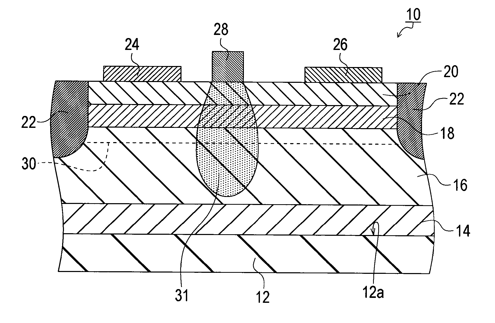
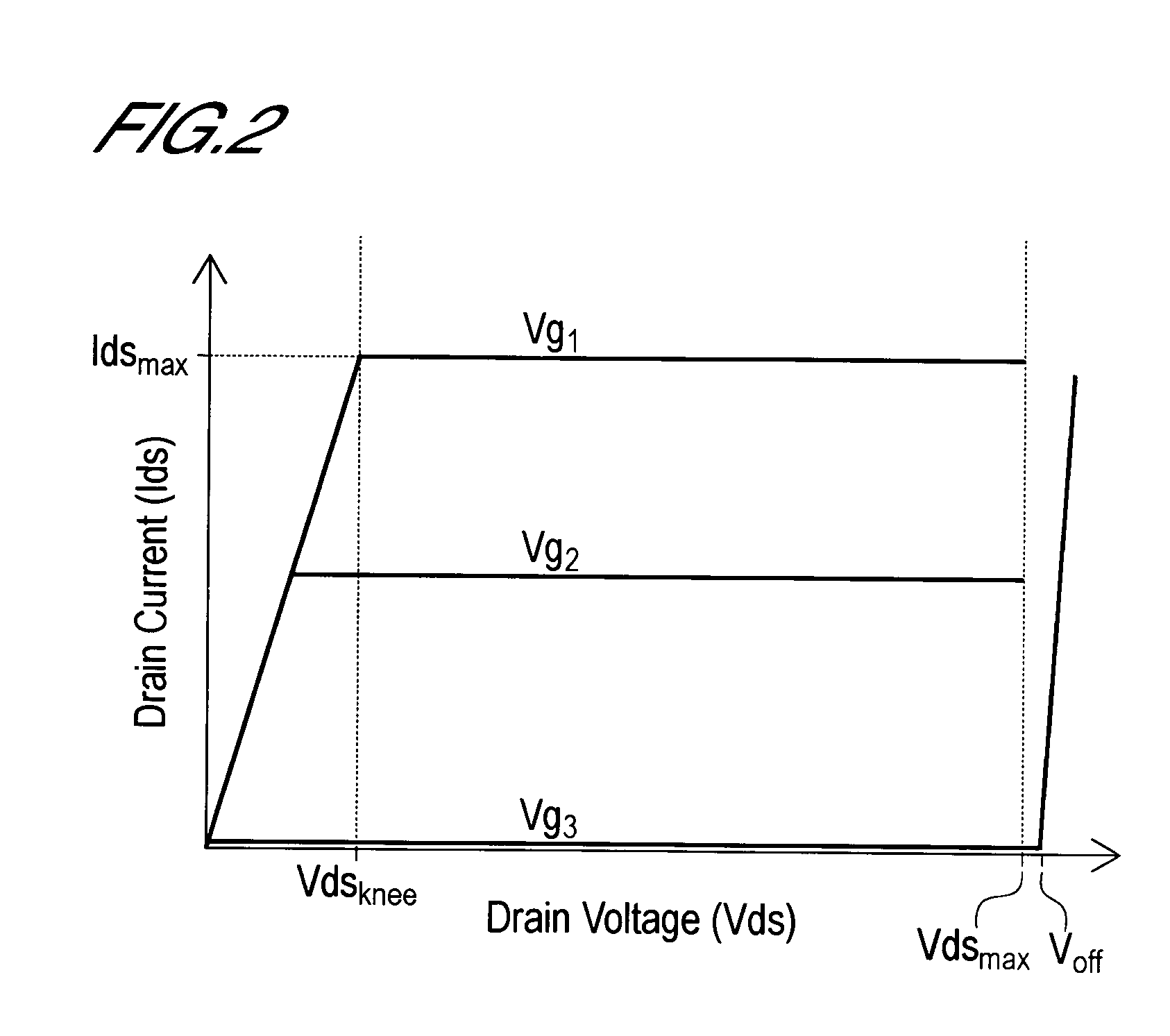
[0036] The structure and operation of the HEMT of a first embodiment are explained referring to FIG. 1 through FIG. 8. FIG. 1 is a schematic sectional view showing the cross-sectional structure of the HEMT. FIG. 2 shows the relation between the drain voltage and drain current (hereafter called the “I-V characteristic”). FIG. 3 shows a cross-section used to explain basic operation of the HEMT. FIG. 4A through FIG. 4C show I-V characteristics used to explain the specific operation of the HEMT. FIG. 5A through FIG. 5C are used to explain the off-state breakdown voltage of the HEMT. FIG. 6 shows the relation between film thickness and off-state breakdown voltage for the HEMT. FIG. 7A and FIG. 7B show cross-sections obtained at respective stages of main processes, to explain the processes of manufacture of the HEMT. FIG. 8A and FIG. 8B show cross-sections obtained at respective stages of main processes, to explain the processes of manufacture of the HEMT.

[0037] The configuration example...

second embodiment

[0095] The structure and operation of a wafer for semiconductor device fabrication of a second embodiment are explained, referring to FIG. 9. FIG. 9 is a schematic sectional view showing the cross-sectional structure of a second embodiment of the wafer for semiconductor device fabrication.

[0096] The wafer 40 for semiconductor device fabrication of the second embodiment has the same structure as the wafer 32 for semiconductor device fabrication explained in the first embodiment, except for two differences, which are the provision, on the buffer layer 14, of an AlGaN layer as a second buffer layer 42, and the provision, on the second buffer layer 42, of a superlattice 44 in which AlN layers and GaN layers are stacked in alternation. Here, the same symbols are assigned to constituent components common to the wafer 32 for semiconductor device fabrication, and explanations thereof are omitted.

[0097] The wafer 40 for semiconductor device fabrication comprises a substrate 12, of semi-ins...


PUM


Abstract

A wafer for semiconductor device fabrication, from which large output power can be obtained by making the off-state breakdown voltage higher than in the prior art. The wafer for semiconductor device fabrication comprises a substrate, GaN electron transit layer formed on the side of the principal surface of the substrate, and AlGaN electron supply layer formed on the electron transit layer. The thickness of the electron transit layer is from 0.2 to 0.9 μm.

Description

BACKGROUND OF THE INVENTION [0001] 1. Field of the Invention [0002] This invention relates to a wafer suitable for use in semiconductor device fabrication, method of manufacturing a wafer, and a field effect transistor. [0003] 2. Description of Related Art [0004] Gallium nitride semiconductors (hereafter “GaN semiconductors”) have properties of a high dielectric breakdown voltage and high saturation electron velocity. HEMTs (high-speed mobility transistors) comprising AlGaN / GaN heterostructures, which utilize these properties, are attracting attention as high-speed devices to replace GaAs semiconductor devices. [0005] At present, GaN single-crystal substrates are extremely expensive. Hence GaN semiconductors are formed on substrate such, for example, as SiC substrates or sapphire substrates, which are extremely inexpensive and have lattice constants close to those of GaN. Instances of fabrication of GaN semiconductors on more easily obtained Si substrates have also been reported in ...

Claims


Application Information

Patent Timeline
Patent Type & Authority Applications(United States)
IPC IPC(8): H01L29/739H01L21/336
CPCH01L21/02378H01L21/02381H01L21/0242H01L21/02458H01L21/0254H01L21/0262H01L29/2003H01L29/66462H01L29/7787
Inventor MITA, JUROOKITA, HIDEYUKITODA, FUMIHIKO
Owner OKI ELECTRIC IND CO LTD
Why Eureka
Try Eureka