Method of driving solid-state imaging device, solid-state imaging device and camera

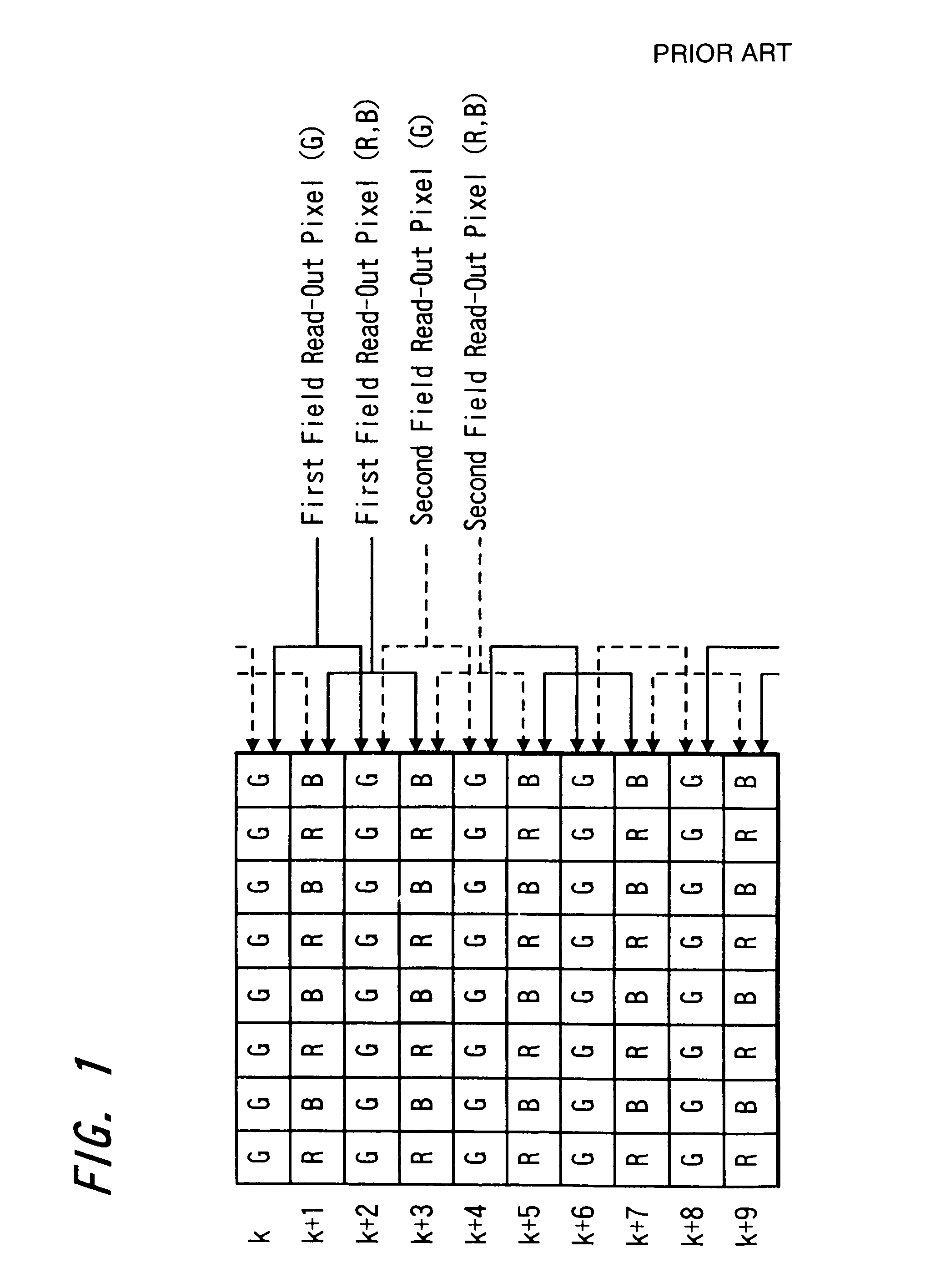
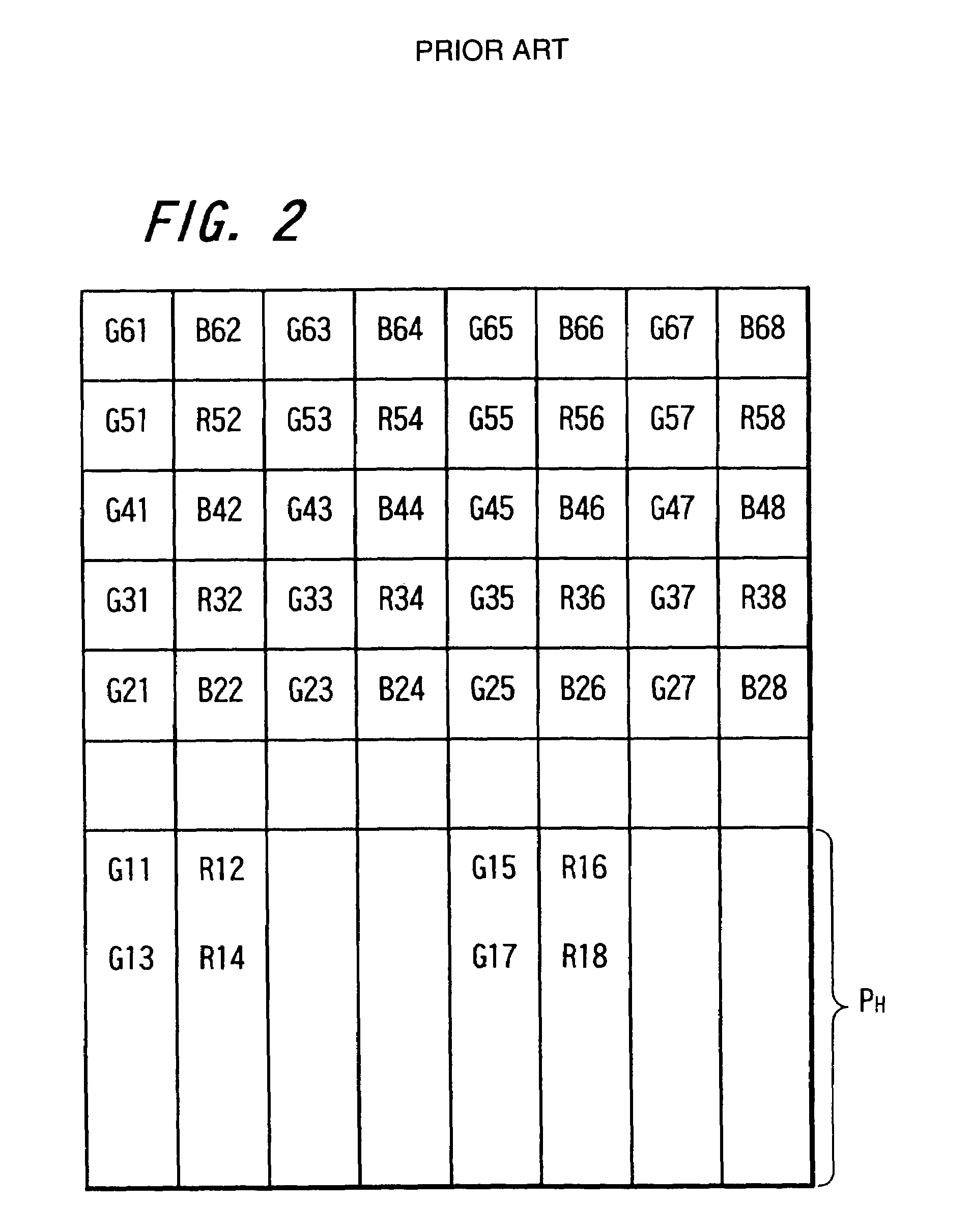
a solid-state imaging and imaging device technology, applied in the direction of picture signal generators, television system scanning details, television systems, etc., can solve the problems of deteriorating balance between horizontal and vertical resolutions, useless signals of remaining 250 lines, and further worsening balan

Inactive Publication Date: 2006-02-21
SONY CORP
View PDF15 Cites 39 Cited by
  • Summary
  • Abstract
  • Description
  • Claims
  • Application Information

AI Technical Summary

Benefits of technology

[0031]In order to solve the above-mentioned problem, according to the present invention, there are provided a solid-state imaging device driving method, a solid-state imaging device and a camera in which the solid-state imaging device is able to operate at a high speed without a change of an angle of view and without a mixture of colors in a color solid-state imaging device by reducing an amount of data in the horizontal direction to ½.
[0036]According to the above-mentioned solid-state imaging device driving method of the present invention, since signal electric charges of pixels distant from each other on the same row are transferred to the horizontal register, the signal electric charges are mixed within the horizontal register and the mixed signal electric charge is transferred in the horizontal direction, it is possible to reduce the number of data in the horizontal direction.
[0037]According to the above-mentioned solid-state imaging device driving method of the present invention, since signal electric charges of pixels of the same color distant from each other on the same row are transferred to the horizontal register, signal electric charges are mixed within the horizontal register and the mixed signal electric charge is transferred in the horizontal direction, the number of data in the horizontal direction may be reduced without generating the mixture of colors.

Problems solved by technology

However, according to the above-mentioned method, when a user views an object by an electronic viewfinder, signals of remaining 250 lines are useless and discarded.
However, in the square lattice pixel, a balance between resolutions in the horizontal and vertical directions is deteriorated.
Also, if the number of data of one frame is further reduced with application of this method, then such balance becomes worse further.
In this method, since the horizontal CCD register should be driven at a higher frequency, a horizontal CCD register with a high frequency and an excellent transfer efficiency becomes necessary, thereby making a design become more difficult.
Further, since only electric charges equivalent to ½ of the number of pixels are used and remaining ½ electric charges are discharged, it is impossible to reduce the number in which the horizontal CCD register transfers signal charges.
This means that the power consumption of the horizontal CCD register becomes twice when a twice frame rate is obtained by discharging ½ electric charges in the horizontal direction, for example.
Also, since ½ signal charges are discharged, an incident light can not be utilized effectively.
However, since the driving frequency of the horizontal CCD should be increased twice in order to increase the frame rate twice, there is then the defect that the power consumption of the horizontal CCD register becomes twice.
Also, since the driving frequency of the horizontal CCD register and the reset frequency of the floating diffusion amplifier are different from each other, a noise caused by a capacitive coupling tends to be mixed into the solid-state imaging device.
In addition, since the output signal of the pixel signal is separated into a first pixel signal and an added signal of first and second pixels, a sampling possible time due to the output signal being flat is reduced to about ½. Thus, the conventional solid-state imaging device is not suitable as a high-speed solid-state imaging device.

Method used


Image

  • Method of driving solid-state imaging device, solid-state imaging device and camera
  • Method of driving solid-state imaging device, solid-state imaging device and camera
  • Method of driving solid-state imaging device, solid-state imaging device and camera

Examples


Embodiment Construction

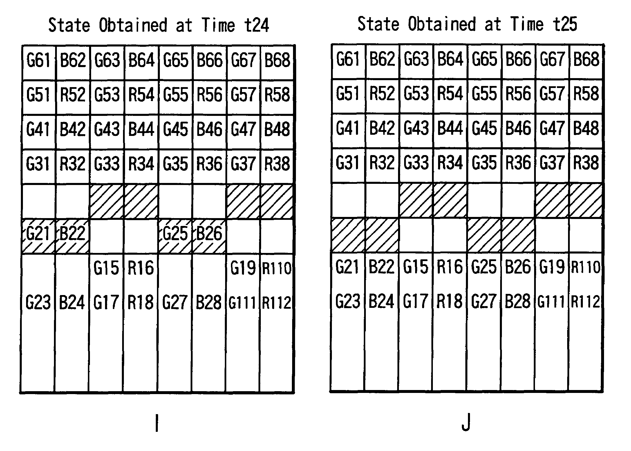
[0059]According to the present invention, in a solid-state imaging device of a two-dimensional array having a pixel comprising a light-receiving accumulation unit and a vertical register (interline transfer type or frame interline transfer type) or a vertical register (frame transfer type) having a light-receiving function and a horizontal register, there is provided a solid-state imaging device driving method which is comprised of the steps of transferring signal charges of pixels distant from each other on the same row to the horizontal register, and mixing the signal charges within the horizontal register and transferring the mixed signal charge in the horizontal direction.

[0060]Also, according to the present invention, in the above-mentioned solid-state imaging device driving method, after the signal charges of pixels distant from each other on the same row are separately transferred from the vertical register to the horizontal register and one signal charge is transferred to th...


PUM


Abstract

To provide a solid-state imaging device driving method, a solid-state imaging device and a camera in which the solid-state imaging device is able to operate at a high speed without a change of an angle of view and without a mixture of colors in a color solid-state imaging device by reducing an amount of data in the horizontal direction to ½. In a solid-state imaging device of a two-dimensional arrangement having a pixel comprising a light-receiving accumulation unit, a vertical register or a vertical register having a light-receiving function and a horizontal register, signal electric charges of pixels distant from each other on one row are transferred to the horizontal register, these signal electric charges are mixed within the horizontal register, and the mixed signal electric charge is transferred in the horizontal direction.

Description

RELATED APPLICATION DATA[0001]The present application claims priority to Japanese Application No. P10 031461 filed Feb. 13, 1998 which application is incorporated herein by reference to the extent permitted by law.BACKGROUND OF THE INVENTION[0002]1. Field of the Invention[0003]The present invention relates to a method of driving a solid-state imaging device having a CCD register, a solid-state imaging device and a camera having provided with a solid-state imaging device.[0004]2. Description of the Related Art[0005]The number of pixels in a solid-state imaging device remarkably increases in accordance with a progress of recent technologies.[0006]As the number of pixels increases as described above, it is strongly desired to having a function to reduce the number of output data in one frame period according to the need.[0007]As an example of such function, in an electronic still camera, for example, when a user takes a picture, a resolution of a still picture is given a priority so th...

Claims


Application Information

Patent Timeline
Patent Type & Authority Patents(United States)
IPC IPC(8): H04N5/335H04N3/14H01L21/339H01L29/762H04N1/48H04N5/341H04N5/347H04N5/357H04N5/369H04N5/3722H04N5/3725H04N5/3728H04N9/04H04N9/07
CPCH04N1/486H04N9/045H04N3/1562H04N25/441H04N25/46H04N25/73H04N25/134
Inventor IIZUKA, TETSUYA
Owner SONY CORP
Why Eureka
Try Eureka