MOS transistor on an SOI substrate with a body contact and a gate insulating film with variable thickness
a transistor and soi substrate technology, applied in the field of semiconductor devices, can solve the problems of kink generation, breakdown voltage deterioration, and electric potential of the channel formation region not being stabilized, and achieve the effect of quick and stable operation and reduced thickness of the soi layer
- Summary
- Abstract
- Description
- Claims
- Application Information
AI Technical Summary
Benefits of technology
Problems solved by technology
Method used
Image

Examples
first embodiment
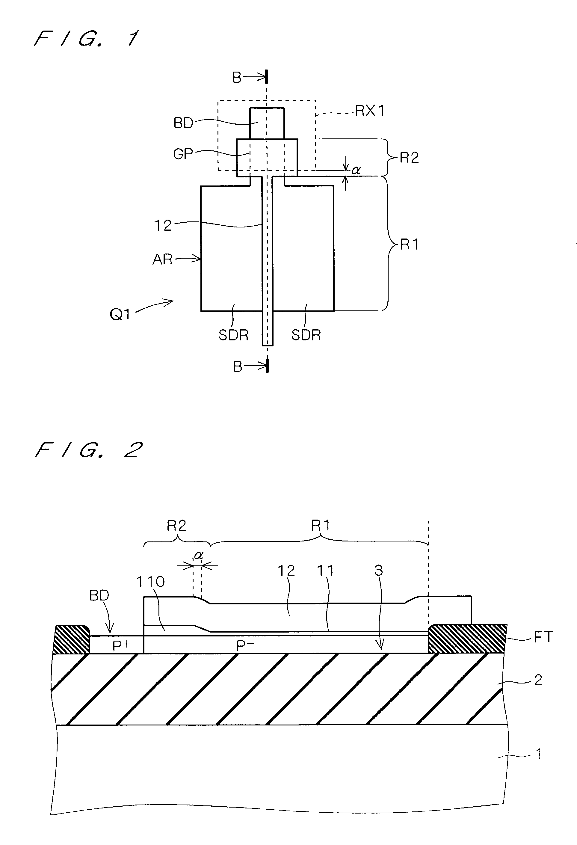
[0062]As a first embodiment according to the present invention, FIG. 1 shows a planar layout of an MOS transistor Q1 having a T-type gate.
[0063]As shown in FIG. 1, the MOS transistor Q1 includes a gate electrode 12 having one of ends in a direction of a gate width which is greatly enlarged in a direction of a gate length and has a T shape seen on a plane.
[0064]A T-shaped head portion of the gate electrode 12 is referred to as a gate contact pad GP and acts as an electrical contact portion for the gate electrode. A body contact portion BD is provided on the outside of a tip of the gate contact pad GP. An impurity region having a reverse conductivity type to that of a source-drain region is formed in a surface of an SOI layer 3 of the body contact portion BD.
[0065]Moreover, an active region AR including a source-drain region SDR and the body contact portion BD are provided continuously, and the gate contact pad GP is provided on the active region AR connecting the source-drain region ...
second embodiment
[0086]As a second embodiment according to the present invention, FIGS. 8 to 11 show planar structures of MOS transistors Q2 to Q5 having a source tie structure.
[0087]In the source tie structure, a band-shaped body contact portion BD is provided in a part of a source region SR and one of ends of the body contact portion BD is connected to a channel region provided under a gate electrode 12. In FIG. 8, in the N-type MOS transistor Q2, the body contact portion BD is provided along the outside of an edge portion of a source region on the opposite side to the side of the gate electrode 12 on which a gate contact pad GP is provided, and an end of the body contact portion BD is connected to the channel region provided under the gate electrode 12. The body contact portion BD has a P conductivity type.
[0088]In FIG. 9, in the P-type MOS transistor Q3, the body contact portion BD is provided along the outside of the edge portion of the source region on the opposite side to the side of the gate...
third embodiment
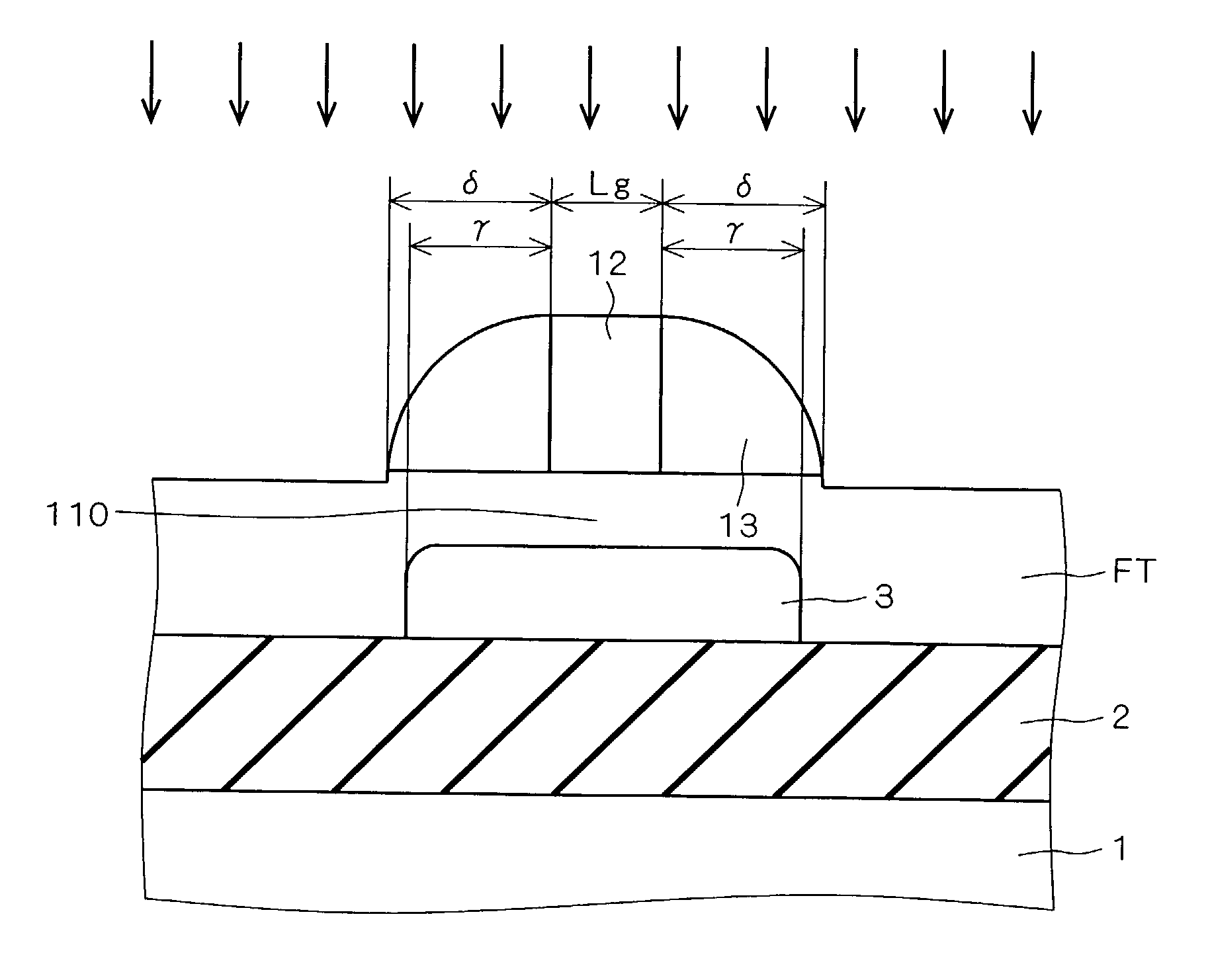
[0097]As a third embodiment according to the present invention, FIG. 12 shows sectional structures of MOS transistors Q11, Q12 and Q13.
[0098]As shown in FIG. 12, the MOS transistors Q11 to Q13 are provided on one SOI substrate constituted by a silicon substrate 1, a buried oxide film 2 and an SOI layer 3.
[0099]In FIG. 12, the MOS transistor Q11 has a gate electrode 12 formed on the SOI layer 3 defined by a perfect trench isolating oxide film FT with a gate insulating film 111 having a comparatively small thickness (for example, a thickness of 1 to 5 nm) provided therebetween.
[0100]Moreover, the MOS transistor Q13 has the gate electrode 12 formed on the SOI layer 3 defined by the perfect trench isolating oxide film FT with a gate insulating film 112 having a comparatively great thickness (for example, a thickness of 3 to 15 nm) provided therebetween.
[0101]The MOS transistor Q12 has such a structure that the gate insulating film 111 having a comparatively small thickness and the gate ...
PUM
 Abstract
Description
Claims
Application Information
 - R&D
- Intellectual Property
- Life Sciences
- Materials
- Tech Scout
- Unparalleled Data Quality
- Higher Quality Content
- 60% Fewer Hallucinations
Browse by: Latest US Patents, China's latest patents, Technical Efficacy Thesaurus, Application Domain, Technology Topic, Popular Technical Reports.
© 2025 PatSnap. All rights reserved.Legal|Privacy policy|Modern Slavery Act Transparency Statement|Sitemap|About US| Contact US: help@patsnap.com