Supercharge Your Innovation With Domain-Expert AI Agents!

Design flow method for integrated circuits

a design flow and integrated circuit technology, applied in the direction of cad circuit design, program control, instruments, etc., can solve the problems of likely timing violation, shorten the time to market for an ic product, improve the efficiency of the ic design process, and effectively control the timing information

Active Publication Date: 2006-02-28
VIA TECH INC
View PDF2 Cites 6 Cited by
  • Summary
  • Abstract
  • Description
  • Claims
  • Application Information

AI Technical Summary

Benefits of technology

[0014]The object of the invention is to shorten the time to market for an IC product by improving the efficiency of IC design process.
[0015]Another object of the invention is to make the DFT synthesis procedure effectively control the timing information, preventing timing violation from happening during the IC design flow process.
[0016]Since the generation of scan chains in the conventional IC design flow process does not take into account the information after placement and routing, timing violation is likely to occur. The invention provides an IC design flow process, wherein the procedure for generating DFT (Design For Test) scan chains includes the information after placement and routing and more accurate timing analysis information. In the disclosed IC design flow process, an IC test is inserted after the placement and routing procedure and the timing analysis. Therefore, during the design flow process the scan chain generation already takes into account the information of placement and routing so that the pre-simulation is unlikely to have timing violation. Furthermore, the IC is ensured to contain no fatal manufacturing errors, increasing the maintainability and error detectability of the system.

Problems solved by technology

Since the generation of scan chains in the conventional IC design flow process does not take into account the information after placement and routing, timing violation is likely to occur.
Therefore, during the design flow process the scan chain generation already takes into account the information of placement and routing so that the pre-simulation is unlikely to have timing violation.

Method used


Image

  • Design flow method for integrated circuits
  • Design flow method for integrated circuits
  • Design flow method for integrated circuits

Examples


Embodiment Construction

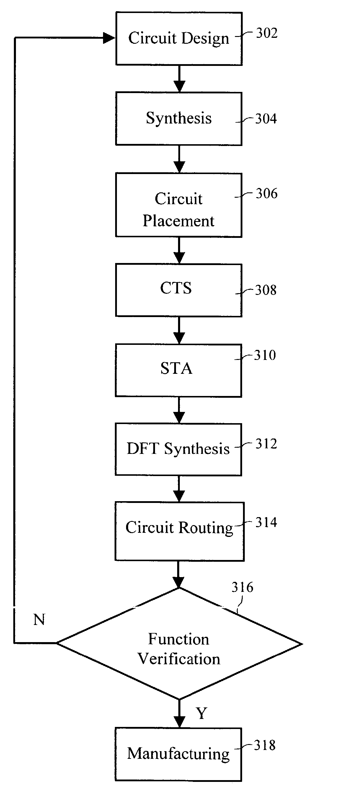
[0023]FIG. 3 shows a flowchart of the design flow method in the present invention, where certain procedures are the same as in FIGS. 1 and 2. The design flow method implemented on IC designs according to the present invention comprising the following procedures:[0024]Step 302, Circuit Design Procedure:

[0025]This procedure generates the function description of circuit modules for the circuitry. In the IC design, a description programming language is used for the function description of the circuitry design in accordance with the specification. A complete description is made according to the desired circuit functions and the internal circuit structure. Each logic cell is converted into a component symbol in the actual circuit. These component symbols are further converted into a circuit analysis simulation program to ensure the design accuracy.[0026]Step 304, Synthesis Procedure:

[0027]This procedure converts the designed circuit modules into the actual gate levels. However, the synthe...


PUM


Abstract

The design flow method of the present invention accurately performs timing analysis during the circuit design stage, so that the DFT synthesis procedure can effectively control the timing information, preventing timing violation from happening during the IC design flow process. Furthermore, the information of the CTS procedure and the static-timing analysis procedure is combined to perform accurate timing estimation.

Description

BACKGROUND OF THE INVENTION[0001]1. Field of Invention[0002]The invention relates to a design flow method, and more particularly, to a circuit design flow method that generates DFT (Design For Test) scan chains for IC implementation.[0003]2. Background of the Invention[0004]The circuit system design of the very large-scale integrated circuit (VLSI) is usually achieved using components provided by a circuit module database. The flow of the IC design contains selecting correct modules and connecting related modules to provide needed functions. The processes for defining the modules are closely related to a database comprising standard cells. Even a small improvement can result in great help in lowering manufacturing costs and enhancing the effects.[0005]Please refer to FIG. 1, which illustrates the links of a scan chain 101 in a circuit module 100. The circuit module 100 is part of a circuitry. In other words, a VLSI includes one or more circuit modules 100. There are functional conne...

Claims


Application Information

Patent Timeline
IPC IPC(8): G06F17/50G01R31/3185
CPCG01R31/318536G06F17/5045G01R31/318594G06F30/30
Inventor YANG, CHUN-CHIHCHIU, YOU-MING
Owner VIA TECH INC
Features
  • R&D
  • Intellectual Property
  • Life Sciences
  • Materials
  • Tech Scout
  • Unparalleled Data Quality
  • Higher Quality Content
  • 60% Fewer Hallucinations
Learn More