Microfluidic devices and methods

a microfluidic and interface technology, applied in the field of microfluidic devices and mass spectrometers, can solve the problems of esi tips being both difficult to manufacture and easy to break or damage, and the microfluidic ms interface structure is difficult to manufacture, and achieves the effect of enhancing the delivery of substances

Inactive Publication Date: 2006-03-07
NORVIEL VERN
View PDF188 Cites 38 Cited by
  • Summary
  • Abstract
  • Description
  • Claims
  • Application Information

AI Technical Summary

Benefits of technology

[0010]Improved microfluidic devices and methods for making and using such devices provide one or more substances to a mass spectrometer for analysis. The microfluidic devices generally include first and second surfaces, at least one microchannel, and an outlet at an edge of the surfaces which is recessed back from an adjacent portion of the edge. Some embodiments include one or more hydrophilic surfaces and / or hydrophobic surfaces to help guide substances out of the outlet to provide the substances to a mass spectrometer in a desired configuration, direction or the like. Some embodiments include a protruding tip that is recessed from the adjacent edge of the surfaces. Such a tip may help guide the substances while remaining resistant to breakage due to its recessed position. To further enhance the delivery of substances, some embodiments include a source of electrical potential to move substances through a microchannel, separate substances and / or provide electrospray ionization.

Problems solved by technology

One drawback of currently available microfluidic MS interface structures is that they typically make use of an ESI tip attached to the microfluidic substrate.
Such ESI tips are both difficult to manufacture and easy to break or damage.
Creating a sharp ESI tip often requires sawing each microfluidic device individually or alternative, equally labor intensive manufacturing processes.
This process can be labor intensive, with precise drilling of a hole in a microfluidic device and insertion of the capillary tube into the hole.
The complexity of this process can make such microfluidic chips expensive, particularly when the microfluidic device is disposable which leads to concern over cross-contamination of substances analyzed on the same chip.
These types of materials, however, are generally not chemically resistant to the organic solvents typically used for electrospray ionization.
Another drawback of current microfluidic devices involve dead volume at the junction of the capillary tube with the rest of the device.
The most practical and cost-effective method currently used to make channels in substrates is isotropic wet chemical etching, which is very limited in the range of shapes it can produce.
Plasma etching of glass or quartz is possible, but is still too slow and expensive to be practical.
Sharp shapes such as a tip cannot readily be produced with isotropic etching, and thus researchers have resorted to inserting fused-silica capillary tubes into glass or quartz chips, as mentioned above.
In addition to being labor-intensive, this configuration can also introduce a certain dead volume at the junction, which will have a negative effect on separations carried out on the chip.
Unfortunately, substances would spread from the opening of the emitter to cover much or all of the edge of the chip, rather than spraying in a desired direction and manner toward an MS device.
This spread along the edge causes problems such as difficulty initiating a spray, high dead volume, and a high flow rate required to sustain a spray.
Another problem sometimes encountered in currently available microfluidic ESI devices is how to apply a potential to substances in a device with a stable ionization current while minimizing dead volume and minimizing or preventing the production of bubbles in the channels or in the droplet at the channel outlet.
The conductive coating, however, often erodes or is otherwise not reproducible.
Furthermore, bubbles are often generated in currently available devices during water electrolysis and / or redox reactions of analytes.
Such bubbles adversely affect the ability of an ESI device to provide substances to a mass spectrometer in the form of a spray having a desired shape.

Method used


Image

  • Microfluidic devices and methods
  • Microfluidic devices and methods
  • Microfluidic devices and methods

Examples


Embodiment Construction

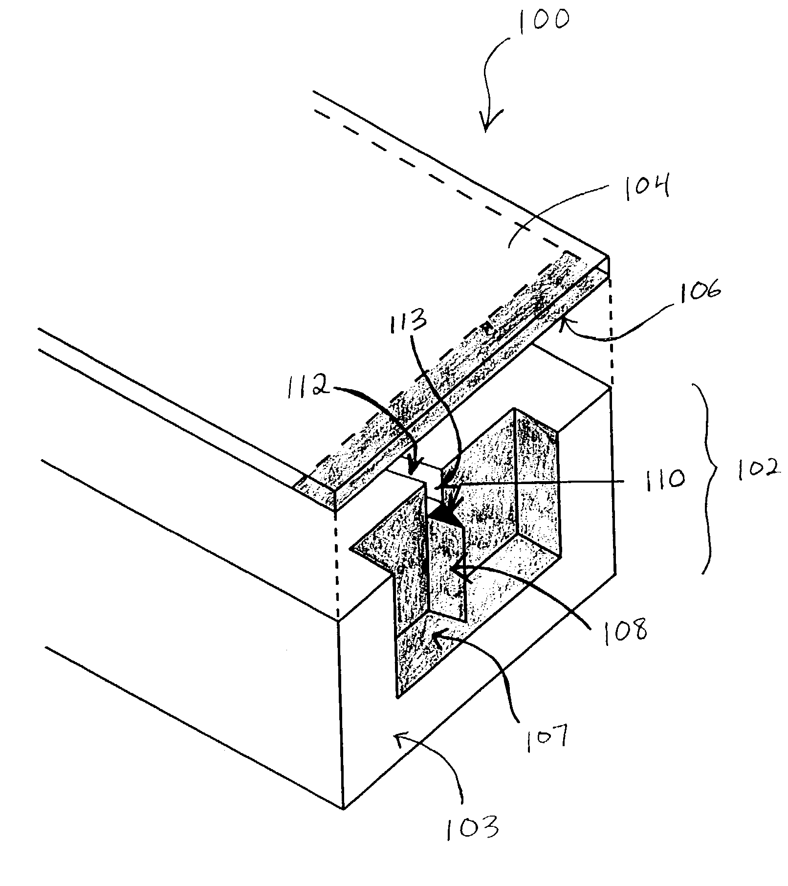
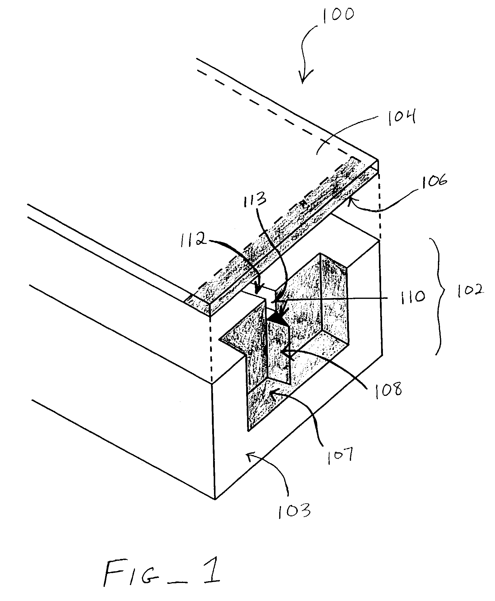
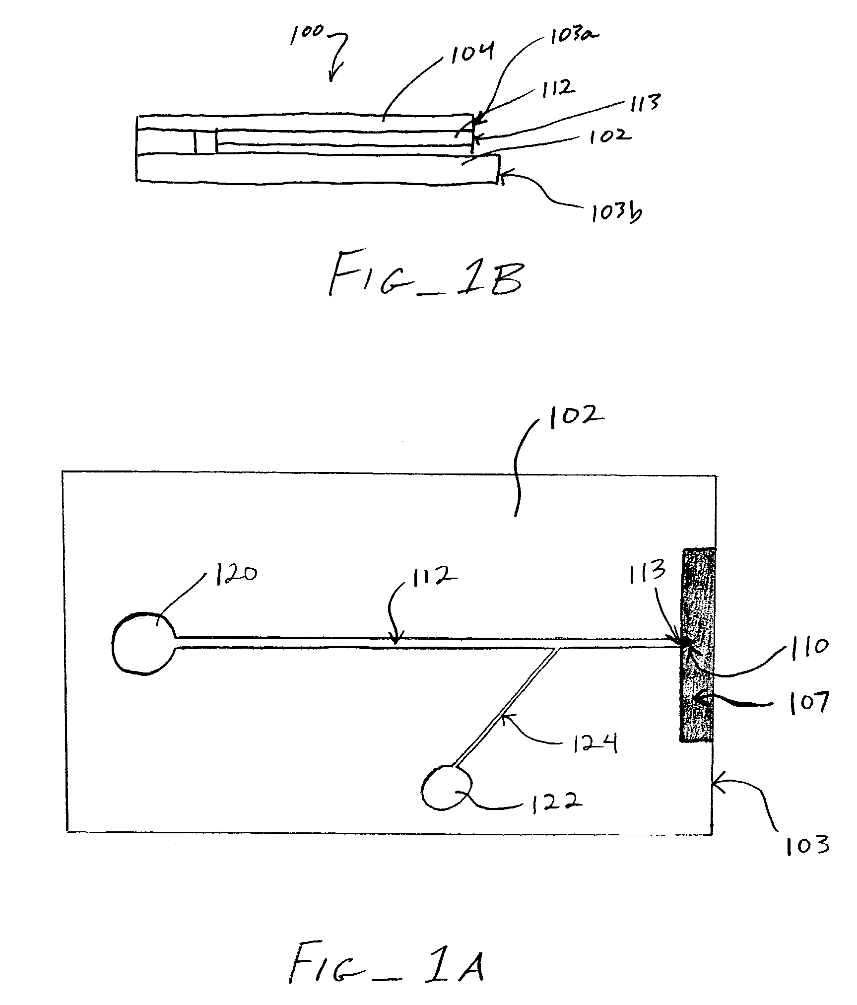
[0041]Improved microfluidic devices and methods for making and using such devices provide one or more substances to a mass spectrometer for analysis. The microfluidic devices generally include first and second surfaces, at least one microchannel formed by the surfaces, and an outlet at an edge of the surfaces which is recessed back from an adjacent portion of the edge. Some embodiments include one or more hydrophilic surfaces and / or hydrophobic surfaces to help guide substances out of the outlet to provide the substances to a mass spectrometer in a desired configuration, direction or the like. Hydrophilic surfaces may minimize or inhibit protein binding, which may also be beneficial, so that alternative surfaces which inhibit protein binding may also be employed in place of the hydrophilic surfaces described herein. Some embodiments include a protruding tip that is recessed from the adjacent edge of the surfaces. Such a tip may help guide the substances while remaining resistant to ...


PUM

PropertyMeasurementUnit
radiusaaaaaaaaaa
diameteraaaaaaaaaa
diameteraaaaaaaaaa

Abstract

Microfluidic devices provide substances to a mass spectrometer. The microfluidic devices include first and second surfaces, at least one microchannel formed by the surfaces, and an outlet at an edge of the surfaces which is recessed back from an adjacent portion of the edge. Hydrophilic surfaces and / or hydrophobic surfaces guide substances out of the outlet. A source of electrical potential can help move substances through the microchannel, separate substances and / or provide electrospray ionization.

Description

BACKGROUND OF THE INVENTION[0001]The present invention relates generally to medical devices and methods, chemical and biological sample manipulation, spectrometry, drug discovery, and related research. More specifically, the invention relates to an interface between microfluidic devices and a mass spectrometer.[0002]The use of microfluidic devices such as microfluidic chips is becoming increasingly common for such applications as analytical chemistry research, medical diagnostics and the like. Microfluidic devices are generally quite promising for applications such as proteomics and genomics, where sample sizes may be very small and analyzed substances very expensive. One way to analyze substances using microfluidic devices is to pass the substances from the devices to a mass spectrometer (MS). Such a technique benefits from an interface between the microfluidic device and the MS, particularly MS systems that employ electrospray ionization (ESI).[0003]Electrospray ionization generat...

Claims


Application Information

Patent Timeline
Patent Type & Authority Patents(United States)
IPC IPC(8): B08B7/00F15B21/00F15C1/04F16L58/04G01NH01J49/04H01J49/16
CPCH01J49/0018H01J49/165Y10T436/2575Y10T137/0402Y10T137/2082Y10T137/2191Y10T137/2224Y10T137/7036
Inventor HELLER, JONATHANSTULTS, JOHNSRINIVASAN, UTHARABOUSSE, LUCZHAO, MINGQI
Owner NORVIEL VERN
Why Eureka
Try Eureka