Selective capping of copper wiring

a technology of selective capping and copper wiring, which is applied in the direction of electrical equipment, semiconductor devices, semiconductor/solid-state device details, etc., can solve the problems of chemical changes to the conductor, adversely affecting the resistivity and other properties of the conductor, and not providing a satisfactory solution at the top of the structure, etc., to achieve the effect of increasing or decreasing the internal diameter

Inactive Publication Date: 2006-03-07
TWITTER INC
View PDF20 Cites 104 Cited by
  • Summary
  • Abstract
  • Description
  • Claims
  • Application Information

AI Technical Summary

Problems solved by technology

The diffusion of such materials would cause chemical changes to the conductor and adversely affect its resistivity and other properties.
Although Damascene integration provides a facile way to protect Cu conductors on the side and at the bottom, it does not provide a satisfactory solution at the top of the structure.
Capping the top of these structures poses more of a challenge due to the desire for planarity between layers in fabricating a multilayer interconnects structure.
Electroless plating has been demonstrated to selectivity deposit on the interconnect; however, this approach offers only a limited set of materials and lacks planarity between layers.
It is apparent that blanket films, even if they address the electromigration and diffusion problems, may cause an unacceptable increase in the overall dielectric constant of the structure.

Method used


Image

  • Selective capping of copper wiring
  • Selective capping of copper wiring
  • Selective capping of copper wiring

Examples


Embodiment Construction

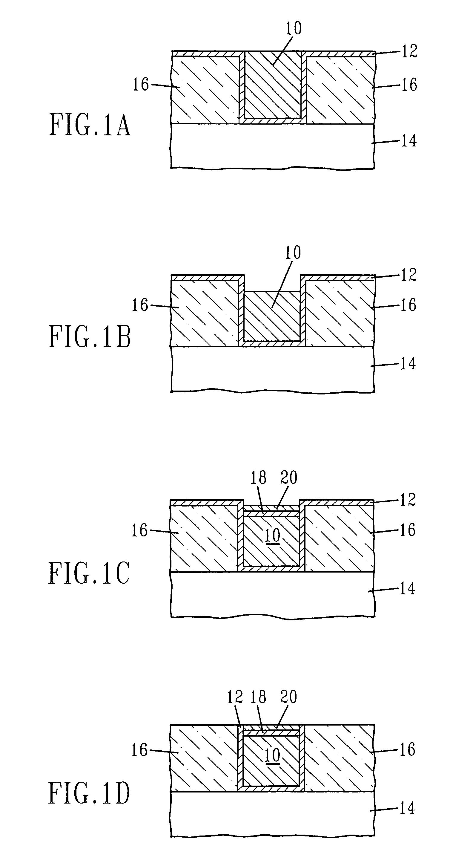
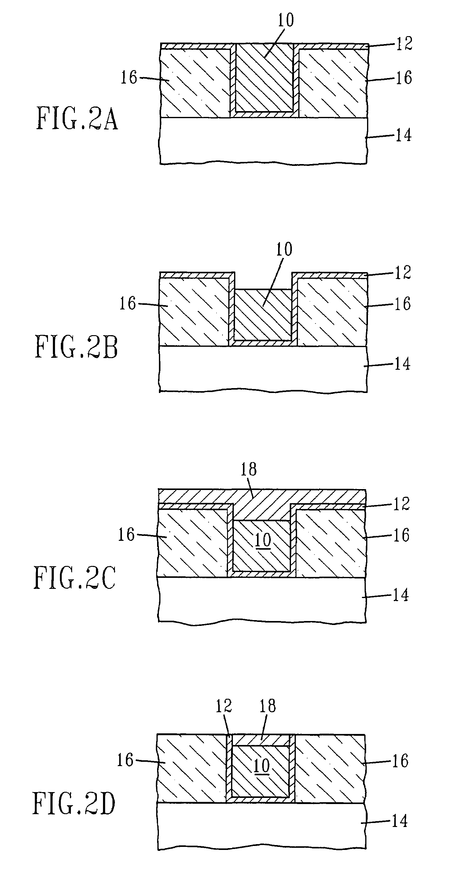
[0032]According to the present invention, copper in the presence of a liner material is selectively capped employing selective etching and / or selective electroplating. According to the present invention, the planarization process employed in a typical process to create a copper structure, such as a damascene or double damascene process, is stopped prior to removal of the liner material. According to the present invention the selective etching and / selectively is carried out in the presence of the liner. This makes possible the elimination of bridging and shorts upon the subsequent removal of the liner.

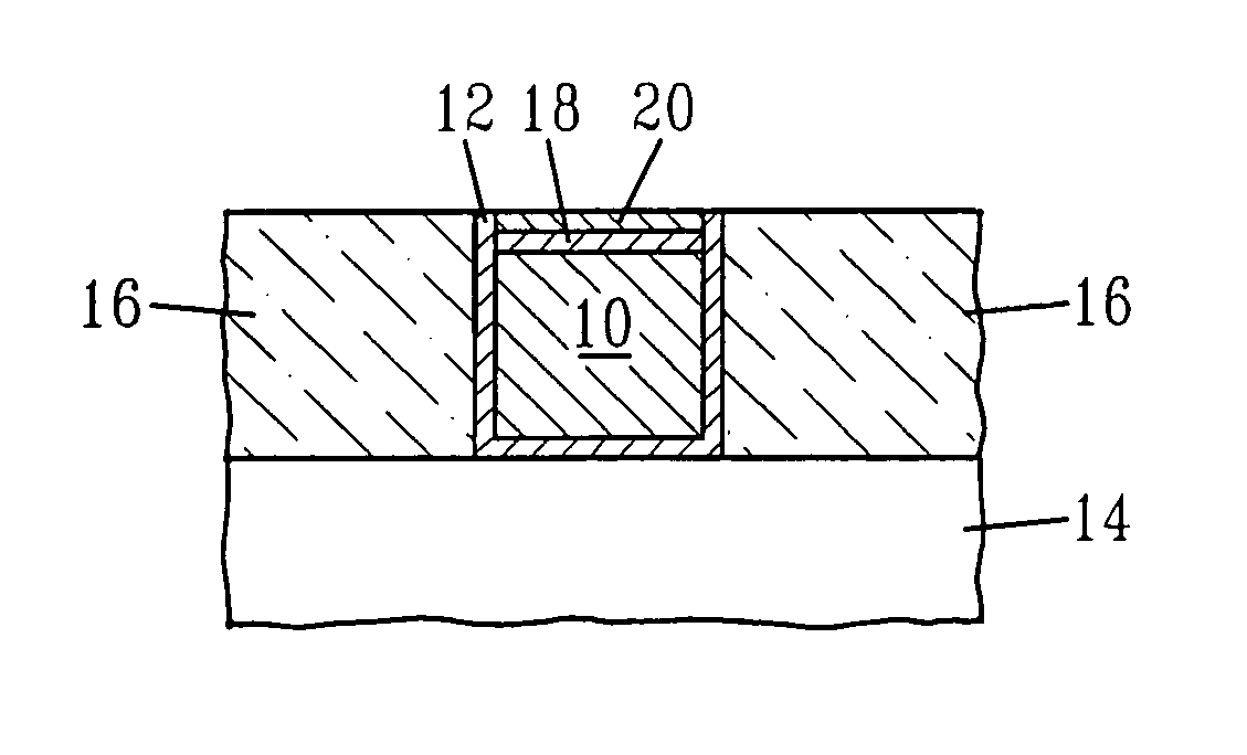
[0033]As illustrated in FIG. 1A, for instance, the wafer surface is then planar and composed of two types of surfaces, the Cu surface 10 and the liner surface 12 (Ta, TaN, W, WN, and the like).

[0034]As will be discussed hereinbelow in detail, the copper surface is selectively etched and / or selectively plated with a capping material. In order to fabricate an understanding of the present ...


PUM

PropertyMeasurementUnit
thicknessaaaaaaaaaa
thicknessaaaaaaaaaa
thicknessaaaaaaaaaa

Abstract

Patterned copper structures are fabricated by selectively capping the copper employing selective etching and / or selective electroplating in the presence of a liner material. Apparatus for addressing the problem of an increased resistive path as electrolyte during electroetching and / or electroplating flows from the wafer edge inwards is provided.

Description

TECHNICAL FIELD[0001]The present invention relates to fabricating patterned copper structures and particularly patterned copper structures wherein the copper is in contact with a liner material. The present invention is concerned with selectively capping the copper employing selective etching and / or selective electroplating. The present invention also relates to apparatus suitable for depositing the capping material on the copper.BACKGROUND OF INVENTION[0002]Copper wiring for on-chip interconnections, currently fabricated by a (single or dual) Damascene integration approach, is surrounded on the sides and at the bottom by a liner or barrier (e.g.—Ta, W, nitrides thereof and multilayers thereof), whose role is to prevent Cu diffusion into the interlayer dielectric material (ILD) (e.g. SiO2 and low k dielectrics) and to provide excellent adhesion between the Cu conductor and the ILD. Additionally, the liner prevents the diffusion of O2 or other substances into the Cu conductor. The di...

Claims


Application Information

Patent Timeline
Patent Type & Authority Patents(United States)
IPC IPC(8): H01L21/44H01L21/00H01L21/288H01L21/768
CPCH01L21/2885H01L21/6708H01L21/76846H01L21/76877H01L21/7685H01L21/76874H01L21/76849H01L21/76883
Inventor ANDRICACOS, PANAYOTIS C.CHEN, SHYNG-TSONGCOTTE, JOHN M.DELIGIANNI, HARIKLIAKRISHNAN, MAHADEVAIYERTSENG, WEI-TSUVEREECKEN, PHILIPPE M.
Owner TWITTER INC
Why Eureka
Try Eureka