This helps you quickly interpret patents by identifying the three key elements:
Problems solved by technology
Method used
Benefits of technology
Problems solved by technology
Further, redundant data is written to the nonvolatile memory in testing the semiconductor integrated circuit mounted therewith.
Method used
Image
Click on the blue label to locate the original text in one second.
Reading with bidirectional positioning of images and text.
Examples
first embodiment
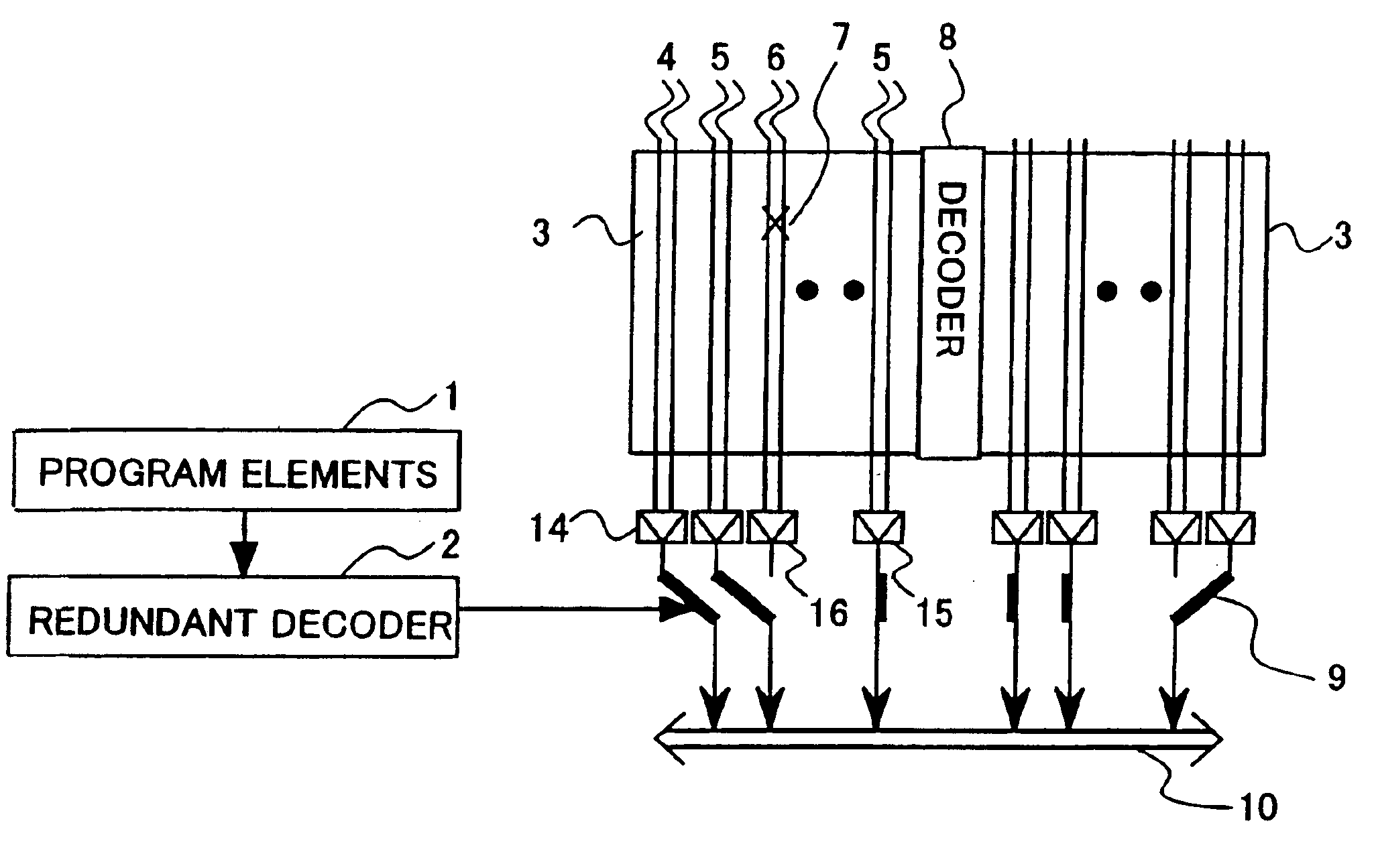
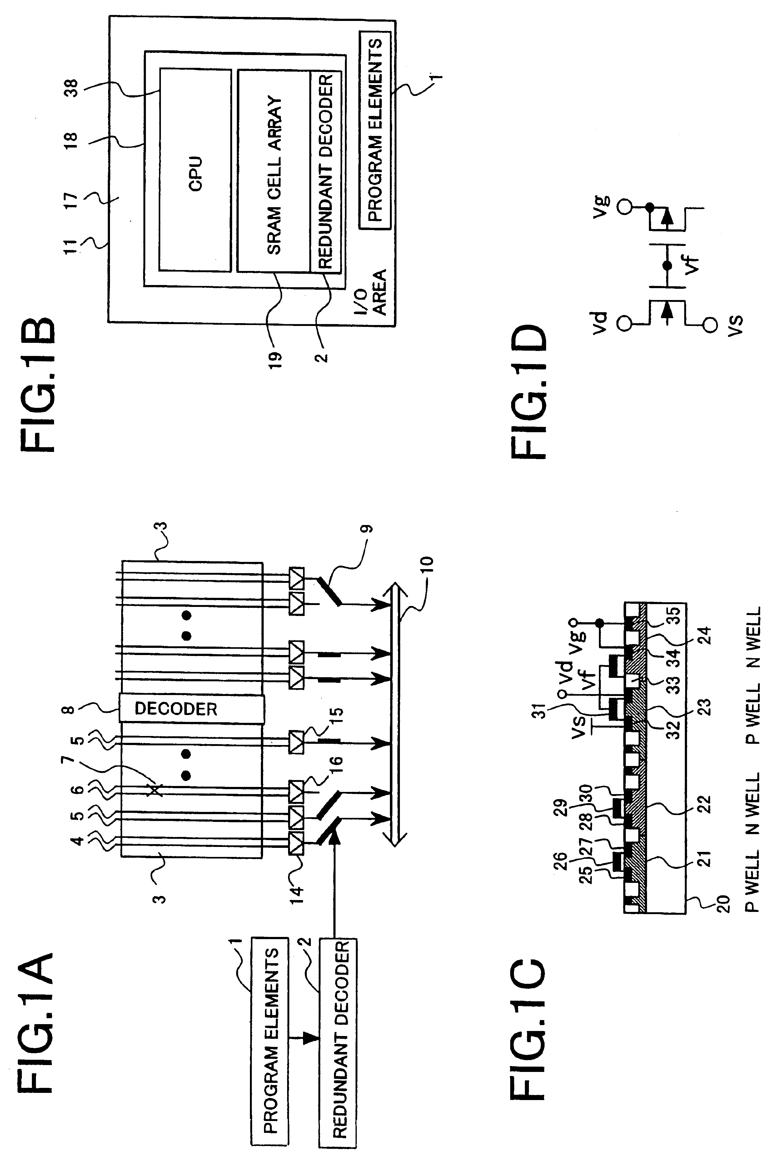
[0039]FIGS. 1A, 1B, 1C and 1D are diagrams showing a FIG. 1A is a schematic diagram of a memory cell array of SRAM having a defect redundancy circuit, FIG. 1B is a block diagram of a chip having the redundancy circuit, FIG. 1C is a sectional view of the chip and FIG. 1D is a circuit diagram of a flash memory.
[0040]In FIG. 1A, numeral 1 designates program elements by flash memories, 2 designates a redundant decoder, 3 designates a memory cell array, 4 designates a redundant bit line, 5 designates a bit line, 6 designates a bit line connected with a memory cell 7 having defect, 8 designates a decoder, 9 designates a switch, 10 designates a buss, 14 designates a sense amplifier for redundancy and numerals 15 and 16 designate sense amplifiers.
[0041]The memory cell array of SRAM is provided with a defect at the memory cell 7 connected to the bit line 6 and the position of the defect is programmed to program elements 1. By reconnecting connection of the switch 9 via the redundancy decode...
second embodiment
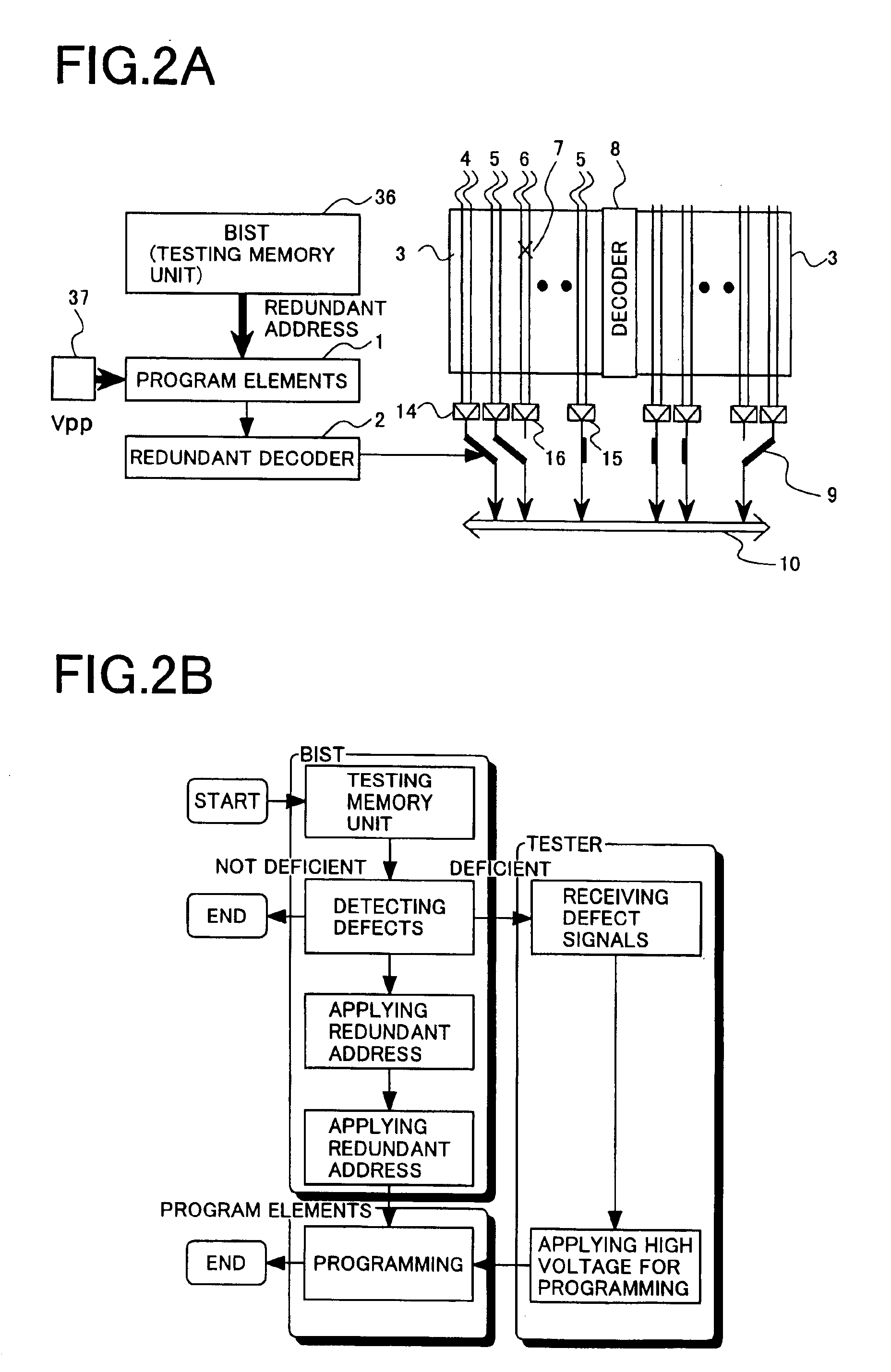
[0050]FIG. 2A is a block diagram according to the invention and FIG. 2B is a flowchart of testing.
[0051]In addition to the constitution of FIG. 1A, there are provided a BIST (Built in Self-Test) circuit block 36 constituting a logic circuit portion having a function of inspecting a cash memory array and Vpp pin 37 constituting a pin for applying high voltage necessary for programming data to a program element.
[0052]The BIST circuit 36 automatically forms a test pattern of a cash memory array to apply to the cash memory cell array and executes inspection of the memory array in a short period of time. Particularly, according to the BIST circuit 36 of the embodiment, there is provided a function of automatically forming redundant address from a result of inspecting the memory cell array.
[0053]According to the embodiment, redundancy is carried out by a testing flow shown by FIG. 2B. After the testing is started, first, it is inspected by the BIST circuit 36 whether the cash memory array...
PUM
Property
Measurement
Unit
voltage
aaaaa
aaaaa
voltage
aaaaa
aaaaa
area
aaaaa
aaaaa
Abstract
To reduce cost of defect redundancy and trimming in a semiconductor integrated circuit having multiple layer wirings and copper wirings, an address for salvaging a defect of a memory cell array in a semiconductor is stored by using a nonvolatile memory element constituting a floating electrode by a first layer of polysilicon, or the nonvolatile memory element is programmed in testing the semiconductor integrated circuit. As a result, a special process is not needed in forming the nonvolatile memory element. In other words, the nonvolatile memory element can be formed in a process of forming a CMOS device and an apparatus of a laser beam for programming is not needed since the programming is carried out in testing. Thus, the time necessary for programming can be shortened, and, therefore, testing costs can be reduced.
Description
CROSS-REFERENCE TO RELATED APPLICATIONS[0001]This application is a Continuation application, of U.S. patent application Ser. No. 09 / 780,393, filed Feb. 12, 2001 now U.S. Pat. No. 6,611,458, the entire disclosure of which is hereby incorporated by reference.FIELD OF THE INVENTION[0002]The present invention relates to a semiconductor integrated circuit device, particularly to a semiconductor integrated circuit device preferable for carrying out defect redundancy of a memory cell array without increasing fabrication cost in a highly-integrated semiconductor integrated circuit using multiple layer wirings.BACKGROUND OF THE INVENTION[0003]Conventionally, in defect redundancy in multiple layer wirings, as a system of programming a location where the defect is disposed, there has been used a method of cutting polysilicon by laser beam or a method of cutting wirings by laser beam. The method is as described in an example executed in DRAM of IEEE International Solid-State Circuits Conference...
Claims
Application Information
Patent Timeline
Application Date:The date an application was filed.
Publication Date:The date a patent or application was officially published.
First Publication Date:The earliest publication date of a patent with the same application number.
Issue Date:Publication date of the patent grant document.
PCT Entry Date:The Entry date of PCT National Phase.
Estimated Expiry Date:The statutory expiry date of a patent right according to the Patent Law, and it is the longest term of protection that the patent right can achieve without the termination of the patent right due to other reasons(Term extension factor has been taken into account ).
Invalid Date:Actual expiry date is based on effective date or publication date of legal transaction data of invalid patent.