Laser processing method, laser welding method, and laser processing apparatus

a laser processing and laser welding technology, applied in the direction of soldering apparatus, manufacturing tools, capacitors, etc., can solve the problems of difficult introduction of laser joining technology into manufacturing settings, difficult to translate a heavy stage in a quick motion according to various directions, and hardly practical stage control, etc., to achieve convenient processing, improve workability and accuracy, and facilitate the effect of handling

Active Publication Date: 2006-03-07
SEIKO EPSON CORP
View PDF9 Cites 64 Cited by
  • Summary
  • Abstract
  • Description
  • Claims
  • Application Information

AI Technical Summary

Benefits of technology

[0009]According to the method, the following effects can be achieved in the processing of a workpiece such as welding, removal, modification, and the like thereof:
[0018]Further, the laser processing apparatus may comprise a solder dispenser for supplying solder to laser irradiation points on the workpiece. With the above arrangement, the laser energy efficiency of solder welding can be improved.

Problems solved by technology

However, the known methods have the following drawbacks.
However, such stage control is hardly practical when it comes to placing the laser welding into mass production lines.
This is because it is terribly difficult to translate a heavy stage in a quick motion according to various directions and intervals of the connecting portions.
In this case, however, a space in which the mirror is placed is necessary in addition to the hardware and software cost of using the galvanometric mirror, which is a negative factor for making it difficult to introduce the laser joining technology into manufacturing settings.
Thus, a problem also arises in that a laser beam utilizing efficiency is rather limited due to the heat dispersion during the irradiation.

Method used


Image

  • Laser processing method, laser welding method, and laser processing apparatus
  • Laser processing method, laser welding method, and laser processing apparatus
  • Laser processing method, laser welding method, and laser processing apparatus

Examples


Embodiment Construction

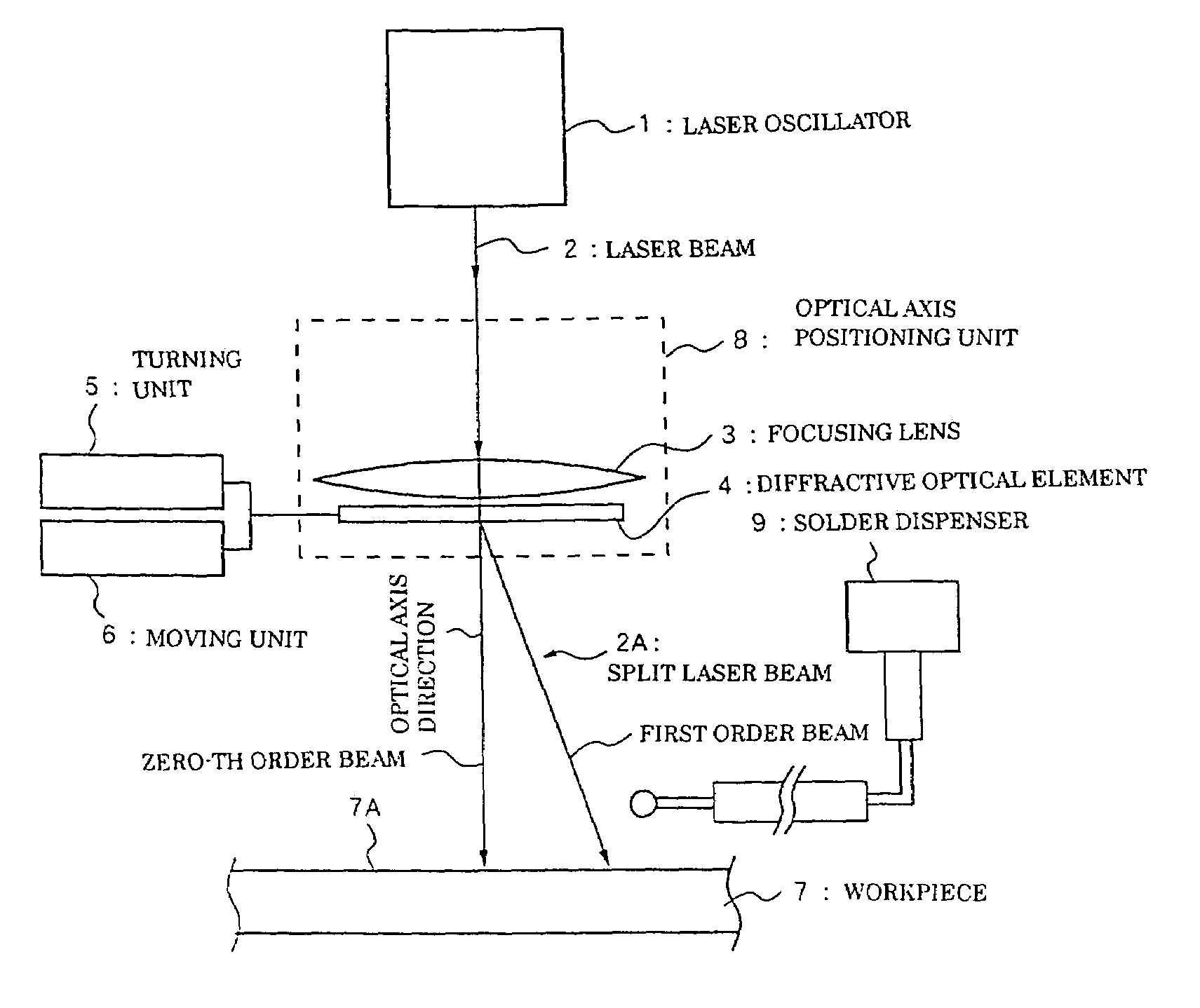
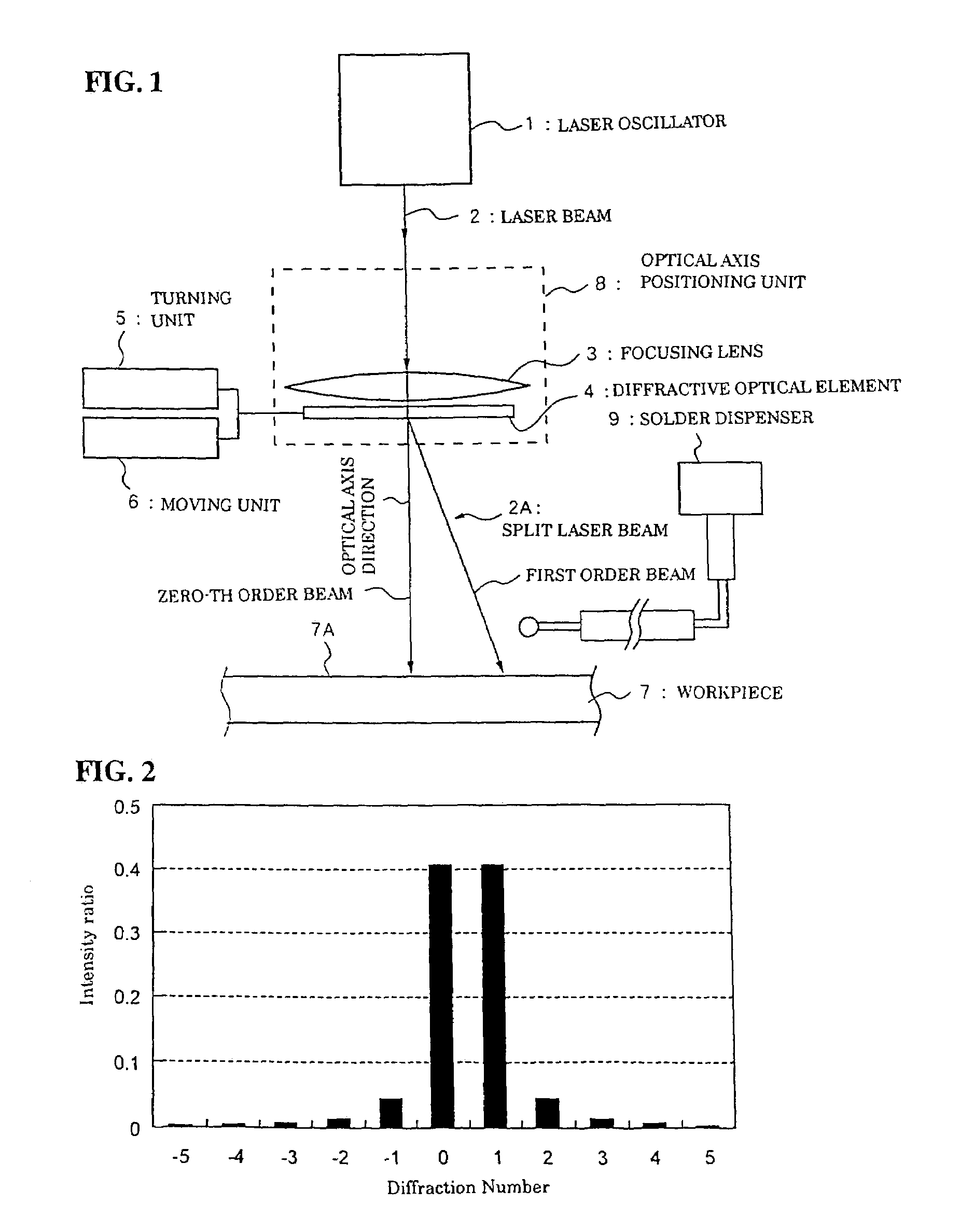
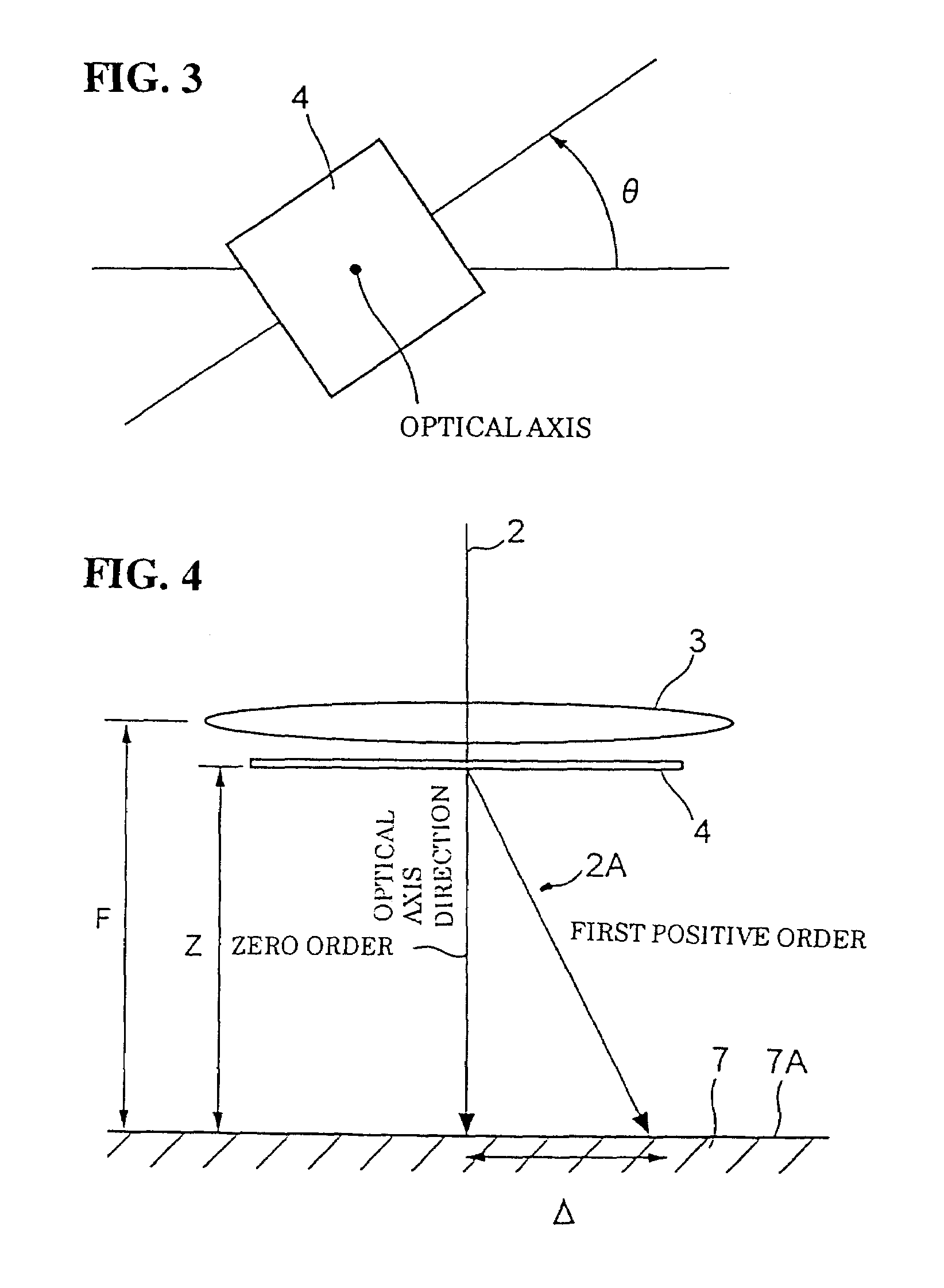
[0027]In the present invention, a zero-order beam is definitely included in an array of focused beam spots (a beam spot array) obtained from a plurality of laser beams (split laser beams) split by a diffractive optical element. The zero-order beam, in principle, is focused on an optical axis regardless of the direction and the length of a beam spot array. Therefore, the zero-order beam can be located at the same position on a processing surface even if the diffractive optical element is turned or its height position is changed on the optical axis. With the above property of the zero-order beam, it is possible to easily adjust the direction and the length of the beam spot array generated by the diffractive optical element by utilizing the position of the zero-order beam as a reference. Note that, in the present invention, it is possible to use the zero-order beam with another order beam or beams, which are arbitrarily chosen. The present invention will be explained below in detail wi...


PUM

PropertyMeasurementUnit
distanceaaaaaaaaaa
wavelengthaaaaaaaaaa

Abstract

A processing method including steps for splitting a single beam into a plurality of beams including a zero-order diffracted beam, by diffracting the single beam by a diffractive element, for turning an array of focused beam spots obtained from the plurality of beams about the center of the zero-order diffracted beam according to the direction of an array of welding points where parts mounted on a circuit board are welded to the board, for causing a spot interval between focused beam spots in the array to agree with the interval between the plurality of welding points by adjusting the distance from the diffractive element to the board, and for increasing the intensity of the plurality of beams, to a welding intensity, and connecting the parts by simultaneously irradiating the welding points with the focused beam spots in the array having the determined direction and spot interval.

Description

BACKGROUND OF THE INVENTION[0001]1. Field of the Invention[0002]The present invention relates to processing using a laser beam, and to, for example, a method of mounting circuit parts on a printed circuit board by solder welding with lead free solder in particular using a laser, and the like.[0003]2. Description of the Related Art[0004]A method of mounting various types of parts (quartz oscillators, ICs, resistors, capacitors, etc.) on a printed circuit board by laser welding with solder is known. Although these various types of the parts are connected to the printed circuit board through the connecting terminals of the parts, the connection terminals of the parts are disposed with variations in orientation and interval. Accordingly, heretofore, the respective parts are connected to the printed circuit board by sequentially laser welding at a plurality of connecting portions in such a manner that connecting portions where solder is deposited are irradiated with a single laser beam o...

Claims


Application Information

Patent Timeline
Patent Type & Authority Patents(United States)
IPC IPC(8): B23K26/22B23K26/067B23K1/005B23K26/042B23K26/064B23K26/21B23K101/38H05K3/34
CPCB23K1/0056B23K26/067B23K26/0676H05K3/3494H05K2203/107B23K26/042
Inventor AMAKO, JUNKAYAMORI, SUSUMU
Owner SEIKO EPSON CORP
Why Eureka
Try Eureka