Small-taper high-quality efficient machining device and method for via holes in surface of packaging substrate

A technology for packaging substrates and via holes, applied in metal processing equipment, manufacturing tools, welding equipment, etc., can solve problems such as laser shielding, scattering, reducing laser energy, and affecting the quality of via holes

Inactive Publication Date: 2021-06-08
XI AN JIAOTONG UNIV
View PDF6 Cites 2 Cited by
  • Summary
  • Abstract
  • Description
  • Claims
  • Application Information

AI Technical Summary

Problems solved by technology

In order to achieve high-density interconnection of electronic systems, it is usually necessary to process arrayed via holes on the surface of the package substrate. Traditional processing methods have been difficult to meet the process requirements of some materials. Laser processing has become the first choice for the manufacture of via holes on package substrates. Way
[0003] Laser processing has the characteristics of high processing efficiency, small surface deformation, no tool loss, and no pollution. It can realize high-precision processing of materials with high hardness, high brittleness, and high melting point. The following defects: when laser drilling, the material in the processing area is directly melted or evaporated under the high-energy laser, and the slag and gasifi

Method used


Image

  • Small-taper high-quality efficient machining device and method for via holes in surface of packaging substrate
  • Small-taper high-quality efficient machining device and method for via holes in surface of packaging substrate
  • Small-taper high-quality efficient machining device and method for via holes in surface of packaging substrate

Examples


Embodiment 1

[0040] Embodiment 1, a high-quality and high-efficiency processing method for small taper via holes on the surface of a packaging substrate, comprising the following steps:

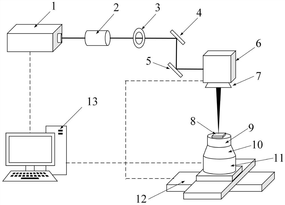
[0041]1) Build an ultrasonic-assisted laser processing system, such as figure 1 As shown, the ultrasonic-assisted laser processing system includes an optical path system and an ultrasonic vibration auxiliary device; the optical path system includes a short-pulse laser 1, and the laser beam output by the short-pulse laser 1 passes through a beam expander 2, a small aperture stop 3, and a first reflecting mirror in sequence. 4. The second reflector 5, the scanning galvanometer 6 and the focusing field mirror 7 act on the packaging substrate, the short pulse laser 1, the beam expander 2, the aperture diaphragm 3, the first reflector 4, and the second reflector 5. The scanning galvanometer 6 and the focusing field lens 7 form an optical path system; the short pulse laser 1 is a nanosecond laser, and the outpu...

Embodiment 2

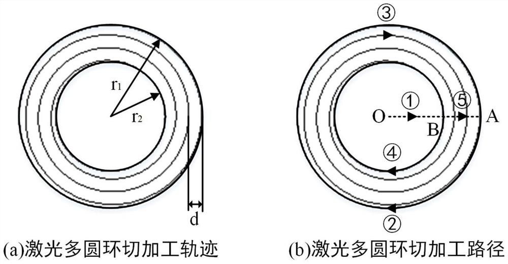
[0055] Example 2: On an alumina ceramic with a thickness of 0.38mm, pre-process a via hole with an inlet diameter of 1000 μm, and change the initial circular pattern radius r in step 6) to 1 Set to 490μm, minimum circle pattern radius r 2 It is set to 390 μm, and the filling distance d is set to 10 μm. The other steps are the same as in Example 1. The relationship between the taper of the processed hole and the processing time is as follows Figure 5 As shown by the solid line in , the hole taper basically reaches saturation when the processing time is 35s, and the saturated hole taper ratio is 5.

Embodiment 3

[0058] Example 3: On an alumina ceramic with a thickness of 0.12mm, pre-process a via hole with an inlet diameter of 1500 μm, and change the initial circular pattern radius r in step 6) to 1 Set to 740μm, minimum circle pattern radius r 2 It is set to 640 μm, and the filling distance d is set to 10 μm. The other steps are the same as in Example 1. The relationship between the taper of the processed hole and the processing time is as follows Figure 6 As shown by the solid line in , the hole taper basically reaches saturation when the processing time is 15s, and the saturated hole taper ratio is 5.


PUM

PropertyMeasurementUnit
Diameteraaaaaaaaaa
Widthaaaaaaaaaa
Thicknessaaaaaaaaaa

Abstract

The invention discloses a small-taper high-quality efficient machining device and method for via holes in the surface of a packaging substrate. According to the method, firstly, an ultrasonic vibration auxiliary laser machining system is built, then the packaging substrate is cleaned and clamped on a clamp for laser drilling, and a precise movement workbench is controlled to focus laser on the upper surface of the packaging substrate; then, the coupling vibration frequency of the packaging substrate is searched through an ultrasonic vibration auxiliary device, and ultrasonic vibration parameters are set; laser processing parameters are set through a computer, a laser scanning track is drawn, and scanning track parameters are set; then, a computer controls a short pulse laser to output laser, an ultrasonic vibration device is started at the same time, and a scanning galvanometer is used for controlling the laser to conduct via hole machining on the packaging substrate along a set path; and after the via holes are machined, the packaging substrate is cleaned to obtain a finished product. According to the method, laser processing is assisted by ultrasonic vibration, and material removal is carried out by adopting a laser multi-ring cutting processing track, so that the taper of the via holes is reduced, and the machining efficiency is greatly improved.

Description

technical field [0001] The invention belongs to the technical field of laser processing of package substrates, and in particular relates to a high-quality and high-efficiency processing method with small taper for via holes on the surface of package substrates. Background technique [0002] The packaging substrate is the carrying and protection platform of microelectronic devices. Ceramic materials, epoxy resin materials and aluminum alloys with excellent thermal conductivity, resistivity, low dielectric constant and sufficient rigidity are usually selected. High-end high-power electronic devices are facing In the process of development in the direction of intelligence, integration, and miniaturization, the upgrading of the technical performance of packaging substrates has put forward higher and higher requirements for the precision processing of substrate materials. In order to achieve high-density interconnection of electronic systems, it is usually necessary to process ar...

Claims


Application Information

Patent Timeline
IPC IPC(8): B23K26/382B23K26/064B23K26/082B23K26/70
CPCB23K26/0643B23K26/064B23K26/082B23K26/382B23K26/702
Inventor 赵万芹梅雪松杨子轩
Owner XI AN JIAOTONG UNIV
Why Eureka
Try Eureka