Production process for semiconductor device

a production process and semiconductor technology, applied in semiconductor devices, semiconductor/solid-state device details, electrical devices, etc., can solve the problems of reducing the production cost of semiconductor chips, and achieve the effect of simplifying the step of forming metal electrodes and reducing costs

Inactive Publication Date: 2006-03-07
ROHM CO LTD
View PDF13 Cites 7 Cited by
  • Summary
  • Abstract
  • Description
  • Claims
  • Application Information

AI Technical Summary

Benefits of technology

[0009]It is an object of the present invention to provide a production process for a semiconductor device which allows for cost reduction by simplifying the step of forming metal electrodes.
[0012]The electrode transfer substrate allows for repetitive formation of the metal electrode portions thereon and, hence, can repeatedly be used for a plurality of semiconductor substrates. Therefore, the production process for the semiconductor device is totally simplified thereby to allow for cost reduction.
[0014]More specifically, the metal electrode portion is formed by depositing the metal material on the seed film on the electrode transfer substrate by plating (electroplating or electroless plating). In this case, the electrode transfer substrate formed with the seed film can be used again for formation of a metal electrode portion for the next semiconductor device immediately after the metal electrode portion is transferred onto the semiconductor substrate. The formation of the metal electrode on the semiconductor substrate is thus achieved by the formation of the metal electrode portion on the electrode transfer substrate by plating and the transfer of the metal electrode portion onto the semiconductor substrate, thereby drastically simplifying the process as compared with the prior art.
[0015]The electrode transfer substrate is preferably covered with a patterning film which exposes therefrom a portion of the seed film in an electrode portion forming position. Thus, the metal electrode material can be deposited only on the properly exposed portion of the seed film. This obviates the need for formation and subsequent removal of a patterning film for pattern-formation of the metal electrode portion on the semiconductor substrate, thereby further simplifying the process.
[0019]In this case, the adhesion between the metal electrode portion and the semiconductor substrate is superior to the adhesion between the metal electrode portion and the seed film. Therefore, when the semiconductor substrate and the electrode transfer substrate are pressed together and then separated from each other, the metal electrode portion can assuredly be transferred onto the semiconductor substrate. Thus, the formation of the metal electrode on the semiconductor substrate can advantageously be achieved.
[0021]With this arrangement, when the electrode transfer substrate is joined with the semiconductor substrate, the semiconductor substrate and the seed film can be viewed from a rear side of the electrode transfer substrate (which is opposite from a side thereof on which the metal electrode portion is formed). Since the seed film is locally present in the electrode portion forming position on the electrode transfer substrate, the electrode transfer substrate can properly be positioned with respect to the semiconductor substrate by monitoring the position of the seed film and an electrode forming position on the semiconductor substrate from the rear side of the electrode transfer substrate by proper image pick-up means. This ensures precise transfer of the metal electrode portion.

Problems solved by technology

As can be understood from the foregoing, the formation of the bumps requires complicated steps such as the formation of the resist film on a wafer-by-wafer basis, so that the process involves an increased number of steps thereby hindering the reduction in the production cost of the semiconductor chip.

Method used


Image

  • Production process for semiconductor device
  • Production process for semiconductor device
  • Production process for semiconductor device

Examples


Embodiment Construction

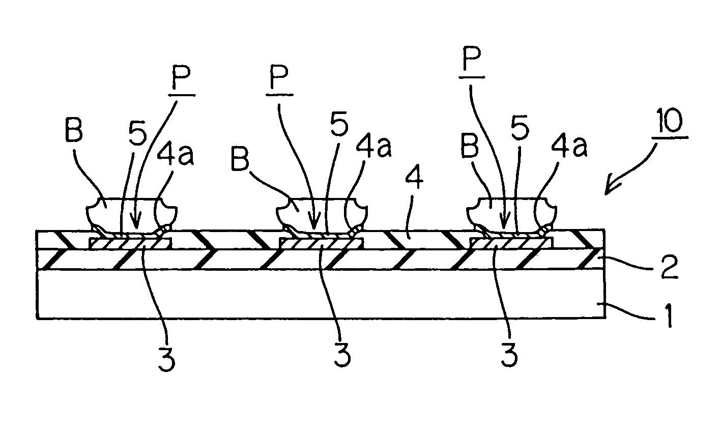
[0032]FIG. 1 is a sectional view illustrating the construction of a semiconductor chip to be produced through a process according to one embodiment of the present invention. The semiconductor chip 10 has a semiconductor substrate 1, an insulating film 2 formed on a surface of the semiconductor substrate 1, aluminum interconnections 3 formed on the insulating film 2, and a protective film 4 covering the aluminum interconnections 3. Openings 4a are formed in the protective film 4 above pads P (electrical contact portion) which are parts of the aluminum interconnections 3. Surface portions of the aluminum interconnections 3 exposed through the openings 4a are respectively covered with barrier metal layers 5 such as of TiW. Bumps B of an oxidation-resistant metal such as gold, palladium, titanium, silver or iridium are respectively provided on the barrier metal layers 5 as projecting therefrom.

[0033]The surface of the semiconductor substrate 1 is a surface on the side of an active surfa...


PUM

PropertyMeasurementUnit
areaaaaaaaaaaa
areasaaaaaaaaaa
adhesion affinityaaaaaaaaaa

Abstract

A production process for a semiconductor device having a metal electrode on a semiconductor substrate thereof. A metal electrode portion is formed on a surface of another substrate for electrode transfer. Then, the metal electrode portion is transferred from the electrode transfer substrate onto the semiconductor substrate by pressing together the electrode transfer substrate and the semiconductor substrate. The electrode transfer substrate has, for example, a seed film provided on the surface thereof, and the formation of the metal electrode portion on the electrode transfer substrate may be achieved by depositing a material for the metal electrode on the seed film by plating. The electrode transfer substrate may have an insulating film which covers a surface of the seed film except a portion thereof on which the metal electrode portion is to be formed.

Description

[0001]This application is a divisional of application Ser. No. 09 / 511,800, which was filed on Feb. 23, 2000 now U.S. Pat. No. 6,696,347.BACKGROUND OF THE INVENTION[0002]1. Field of the Invention[0003]The present invention relates to a production process for a semiconductor device having metal electrodes such as bumps provided on its surface.[0004]2. Description of Related Art[0005]Some of semiconductor chips have metal electrodes such as bumps projecting from a surface thereof. For example, such a semiconductor chip may be mounted on a printed wiring board by flip-chip bonding, or bonded to another semiconductor chip in a stacked relation to form a semiconductor device of chip-on-chip structure.[0006]In general, the semiconductor chip has an insulating film and an aluminum interconnection film provided on a surface of a semiconductor substrate which serves as a base thereof, and connection pads for external electrical connection provided in proper positions on the surface thereof. A...

Claims


Application Information

Patent Timeline
Patent Type & Authority Patents(United States)
IPC IPC(8): H01L23/48H01L21/60H01L21/68
CPCH01L21/6835H01L24/11H01L2224/11334H01L2224/11003H01L2224/1147H01L2224/13099H01L2924/01002H01L2924/01004H01L2924/01013H01L2924/01015H01L2924/01022H01L2924/01032H01L2924/01046H01L2924/01047H01L2924/01074H01L2924/01077H01L2924/01078H01L2924/01079H01L2924/19043H01L2924/01005H01L2924/01006H01L2924/01024H01L2924/01033H01L2924/10329H01L2224/05001H01L2224/05022H01L2224/05572H01L2224/0615H01L2224/05666H01L2924/00014H01L2224/05684H01L2224/05124
Inventor HIKITA, JUNICHISHIBATA, KAZUTAKAUEDA, SHIGEYUKI
Owner ROHM CO LTD
Why Eureka
Try Eureka