Wide band antenna
a wide-band antenna and antenna technology, applied in the direction of antennas, antenna feed intermediates, basic electric elements, etc., can solve the problems of difficult utilization of conventional bowties in communication network systems, and achieve the effect of low cost and small siz
- Summary
- Abstract
- Description
- Claims
- Application Information
AI Technical Summary
Benefits of technology
Problems solved by technology
Method used
Image

Examples
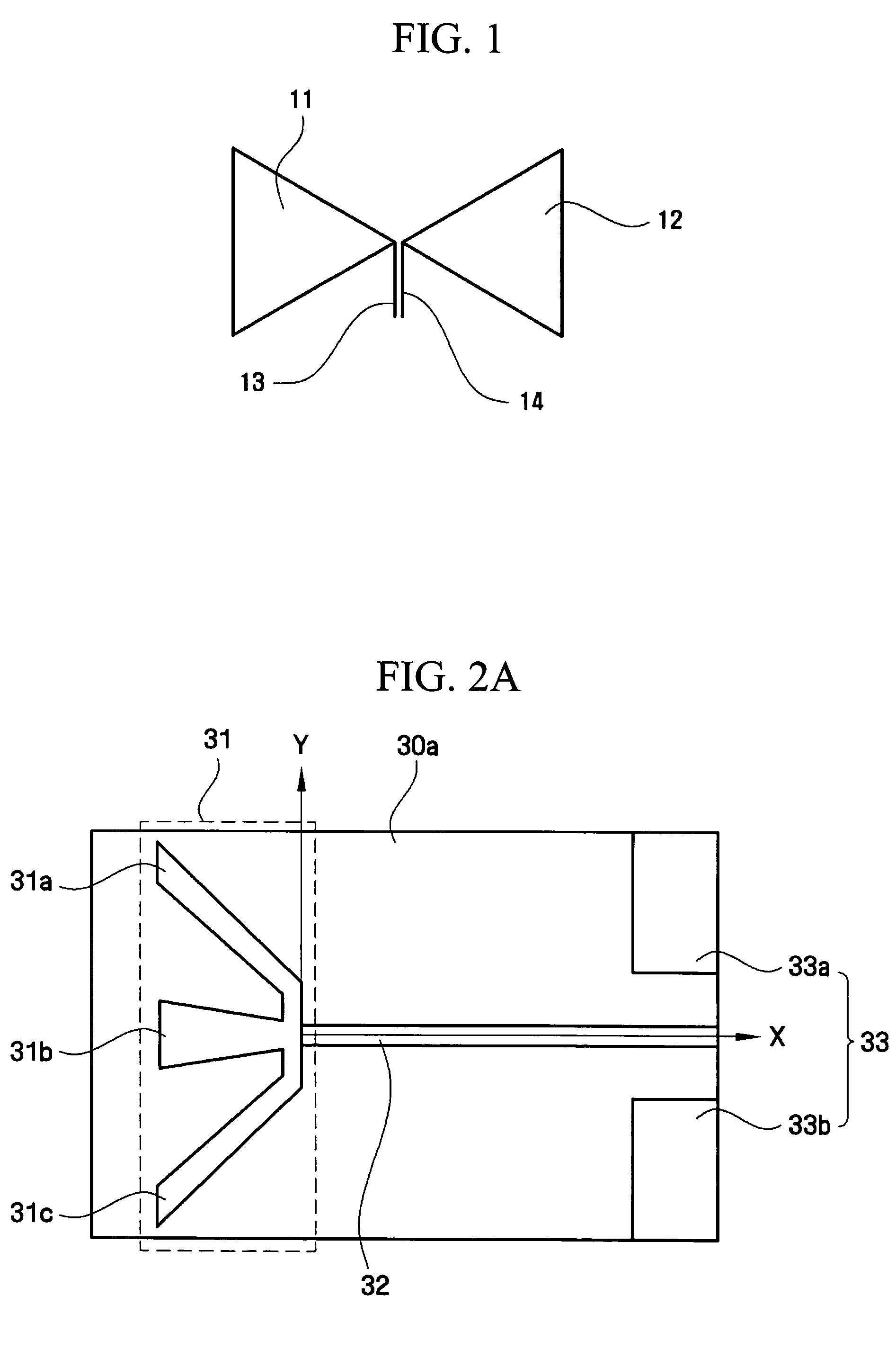
first embodiment
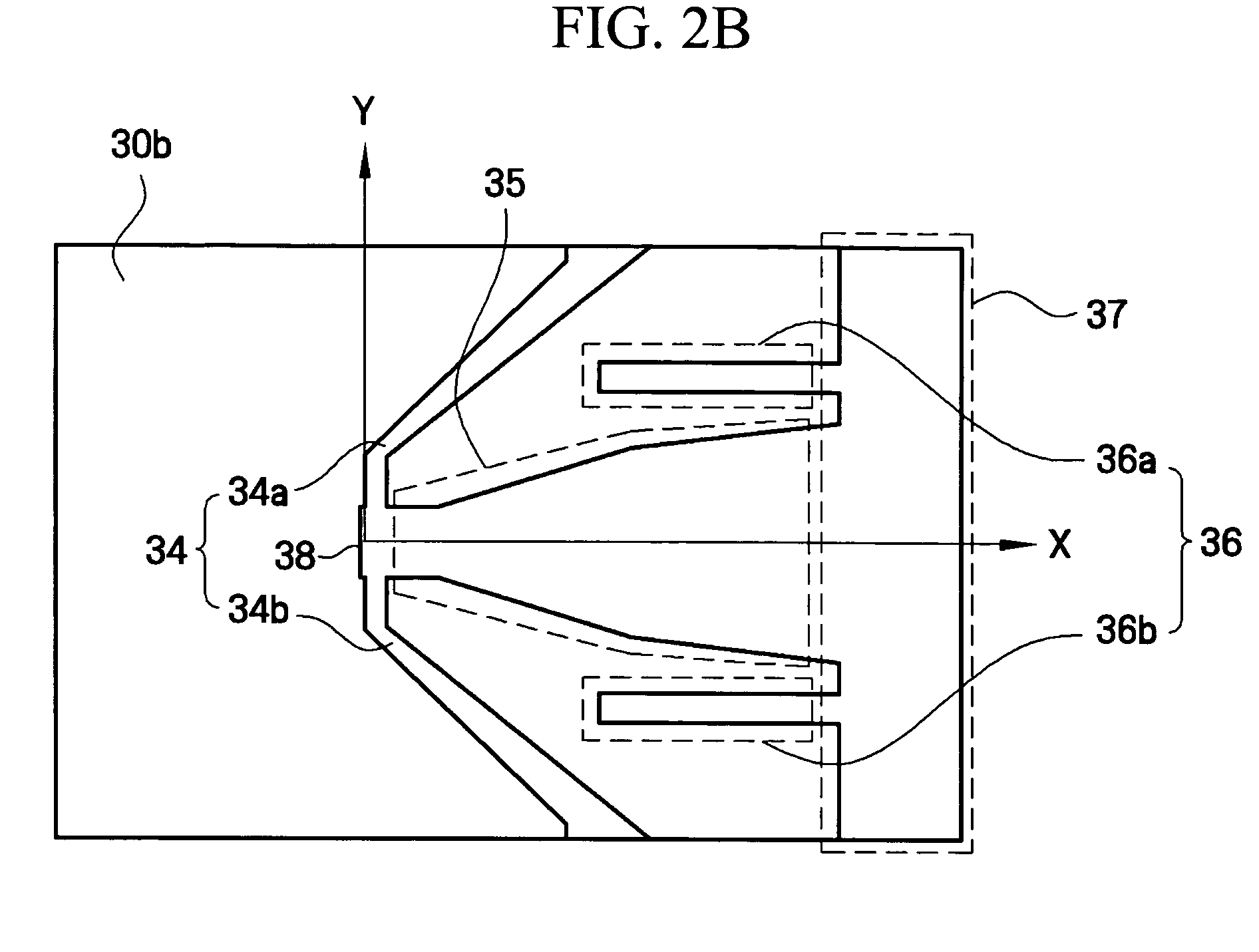
[0027]FIG. 4A illustrates an equivalent circuit of a wide band antenna according to the present invention. The equivalent circuit shown in FIG. 4A correlates to the wide band antenna according to the present invention in the following manner. Circuit elements L1, C1, and R1 represent the first and second antenna units 31 and 34, whereas circuit elements L2, C2, and R2 represent the stub 36. Since one side of the stub 36 is grounded, the resonant circuit comprised of elements L2, C2, and R2 is also grounded. The coupling coefficient M located between L1 and L2 in FIG. 4A represents radiation coupling between the first and second antenna units 31 and 34 and the stub 36. Resistor R3 represents the resistance of an RF signal source, (not shown) which drives the first and second antenna units 31 and 34. Circuit element R1 represents non-radiation losses associated with electromagnetic energy dissipation due to finite conductivity of real conductors in the first and second antenna units 3...
second embodiment
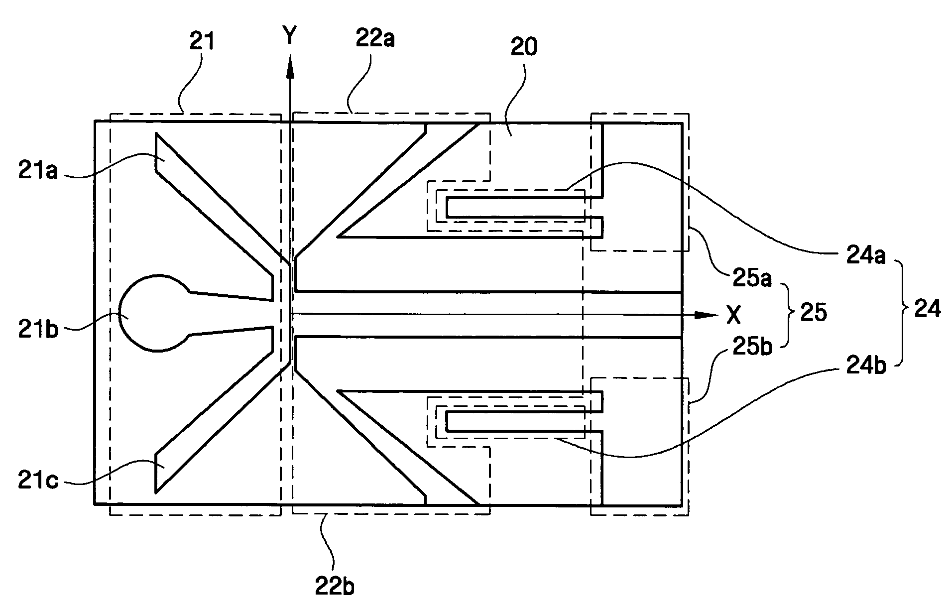
[0038]FIG. 3 is a plane view of a wide band antenna according to the present invention.
[0039]The wide band antenna according to the second embodiment of the present invention includes a first antenna unit 21, a supply cable 23, a connector coupler 25, having couplers 25a and 25b, a second antenna unit 22a, a third antenna unit 22b, and a stub 24.
[0040]The first antenna unit 21 is formed of a metal conductor in a trapezoid shape on a surface 20 of a dielectric substrate. The second antenna unit 22a is formed of a metal conductor on the surface 20 of the dielectric substrate. The second antenna unit 22a includes a first branch, which is formed in a notch shape above the supply cable 23 to be spaced apart from the first antenna unit 21 and the supply cable 23, and a second branch, which is formed in a notch shape above the supply cable 23 to run in parallel with the supply cable 23. The third antenna unit 22b is formed of a metal conductor on the surface 20 of the dielectric substrate....
PUM
 Abstract
Description
Claims
Application Information
 - R&D
- Intellectual Property
- Life Sciences
- Materials
- Tech Scout
- Unparalleled Data Quality
- Higher Quality Content
- 60% Fewer Hallucinations
Browse by: Latest US Patents, China's latest patents, Technical Efficacy Thesaurus, Application Domain, Technology Topic, Popular Technical Reports.
© 2025 PatSnap. All rights reserved.Legal|Privacy policy|Modern Slavery Act Transparency Statement|Sitemap|About US| Contact US: help@patsnap.com