Anodizing method, substrate processing method, and substrate manufacturing method

Inactive Publication Date: 2006-03-21
CANON KK
View PDF24 Cites 38 Cited by
  • Summary
  • Abstract
  • Description
  • Claims
  • Application Information

AI Technical Summary

Benefits of technology

[0014]More specifically, it is an object of the present invention to, e.g., prevent any influence of a gas generated by an anodizing reaction.
[0015]It is another object of the present invention to, e.g., prevent any contamination of a substrate to be processed.
[0016]It is still another object of the present invention to, e.g., increase the speed of a series of processes including anodizing and associated processes.
[0017]It is still another object of the present invention to, e.g., facilitate to cope with an increase in diameter.
[0018]According to the

Problems solved by technology

This makes the porous layer nonuniform to result in p

Method used


Image

  • Anodizing method, substrate processing method, and substrate manufacturing method
  • Anodizing method, substrate processing method, and substrate manufacturing method
  • Anodizing method, substrate processing method, and substrate manufacturing method

Examples


first embodiment

[First Embodiment]

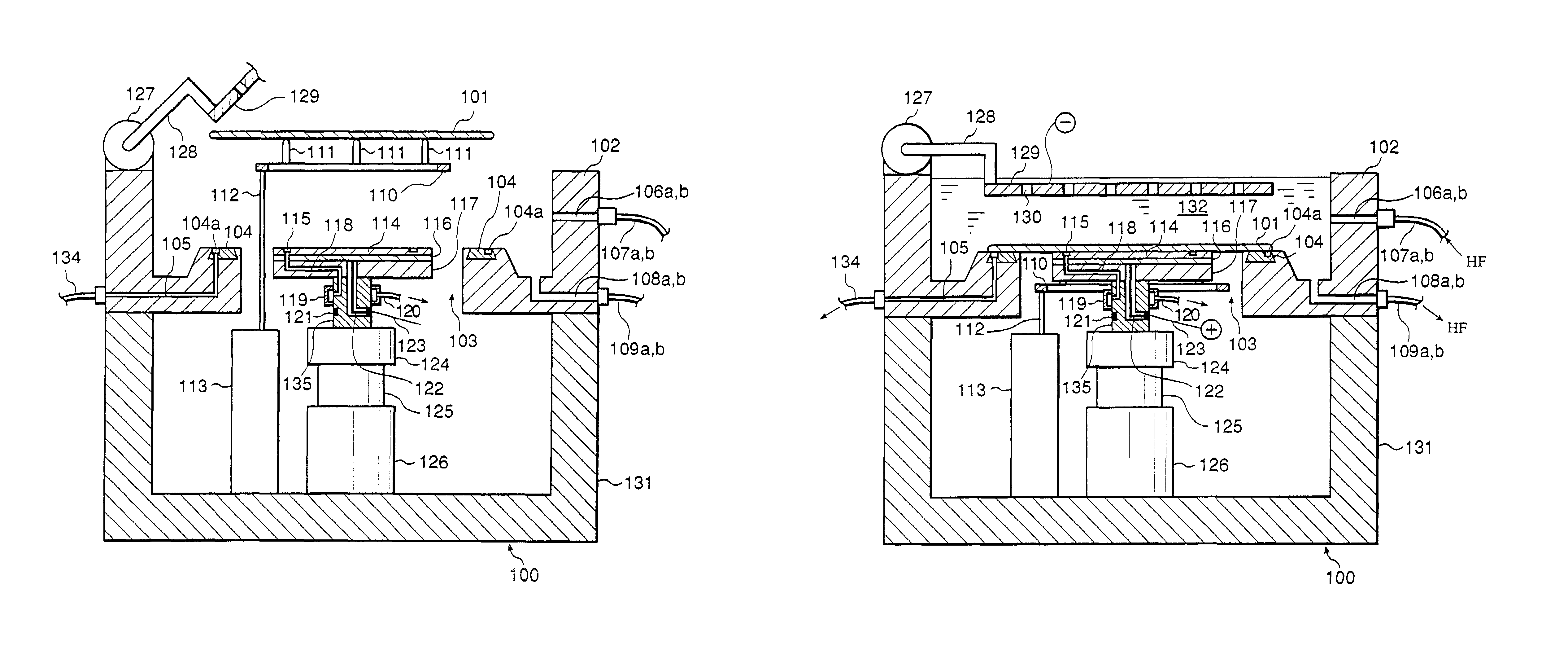
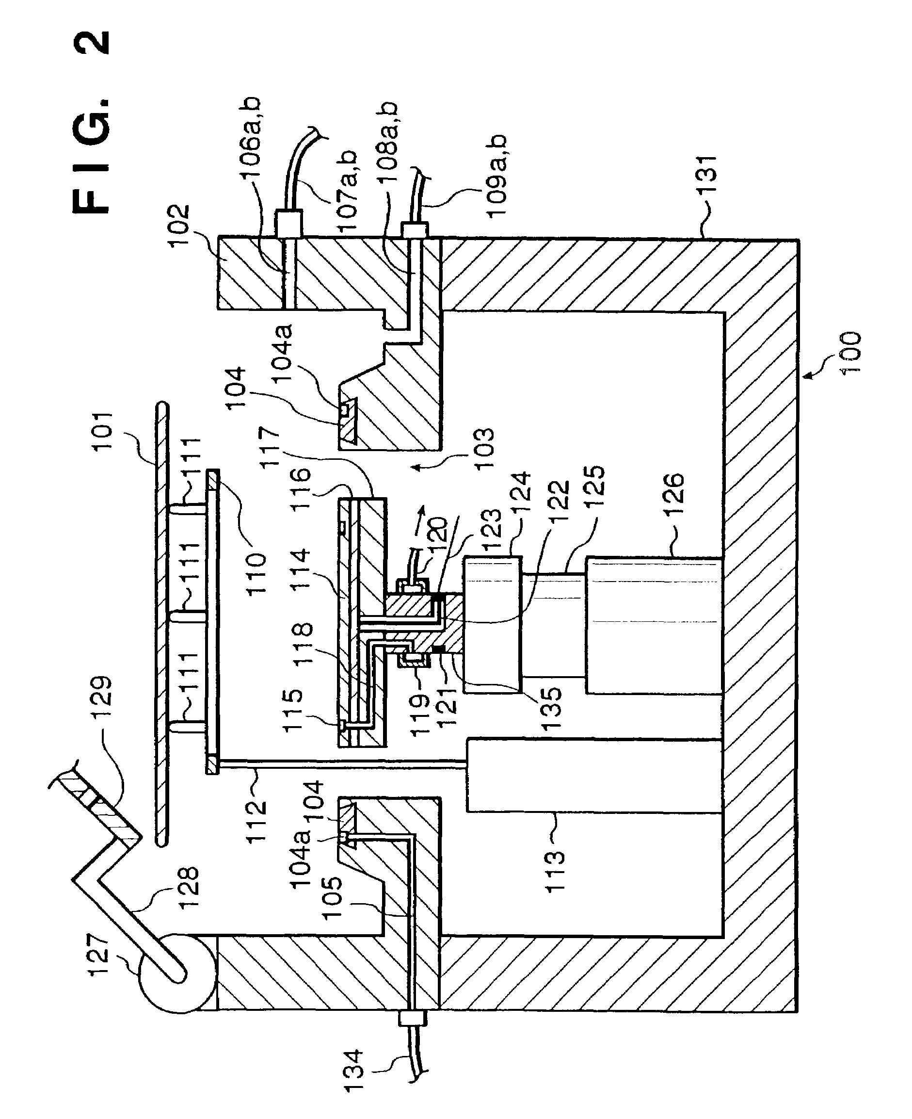
[0102]FIGS. 2 to 9 are views showing the schematic arrangement of an anodizing apparatus according to the first embodiment of the present invention. FIG. 10 is a plan view showing part of an anodizing apparatus 100 shown in FIGS. 2 to 9.

[0103]In the anodizing apparatus 100 according to the first embodiment of the present invention, a series of processes including anodizing, washing, and drying can be executed. According to this anodizing apparatus 100, the substrate need not be conveyed between units for individually performing anodizing, washing, and drying. Hence, for example, 1) the productivity is high, 2) the substrate can be prevented from dropping, and 3) the apparatus can be made compact.

[0104]In the anodizing apparatus 100, the series of processes including anodizing, washing, and drying are performed while horizontally holding a substrate to be processed. Hence, for example, when a substrate is received from a conveyor robot which horizontally holds and c...

second embodiment

[Second Embodiment]

[0152]An automatic anodizing apparatus according to the second embodiment of the present invention will be described below. The automatic anodizing apparatus of this embodiment has an anodizing apparatus 100 according to the first embodiment as an apparatus for performing anodizing, and a separate post-processing apparatus as an apparatus for executing washing and drying.

[0153]FIGS. 13 to 16 are views showing the schematic arrangement of the post-processing apparatus according to the second embodiment of the present invention. FIG. 17 is a plan view showing the schematic arrangement of an anodizing system according to the second embodiment of the present invention.

[0154]The arrangement of a post-processing apparatus 400 according to the preferred embodiment of the present invention will be described first with reference to FIGS. 13 to 16. This post-processing apparatus 400 schematically has the same arrangement as the anodizing apparatus 100 of the first embodimen...


PUM

PropertyMeasurementUnit
Electric potential / voltageaaaaaaaaaa

Abstract

This invention is to reduce the influence of a gas generated by an anodizing reaction. A silicon substrate (101) to be processed is horizontally held. A negative electrode (129) is arranged on the upper side of the silicon substrate (101), and a positive electrode (114) is brought into contact with the lower surface of the silicon substrate (101). The space between the negative electrode (129) and the silicon substrate (101) is filled with an HF solution (132). The negative electrode (129) has a number of degassing holes (130) to prevent a gas generated by the anodizing reaction from staying on the lower side of the negative electrode (129).

Description

[0001]This is divisional of application Ser. No. 09 / 526,869, filed Mar. 16, 2000, now U.S. Pat. No. 6,547,938.FIELD OF THE INVENTION[0002]The present invention relates to an anodizing apparatus, an anodizing system, a substrate processing apparatus and method, and a substrate manufacturing method.BACKGROUND OF THE INVENTION[0003]Porous silicon was found by A. Uhlir and D. R. Turner who were studying electropolishing of single-crystal silicon biased to a positive potential in an aqueous solution of hydrofluoric acid.[0004]Later, to exploit excellent reactivity of porous silicon, application of porous silicon to the element isolation process in manufacturing a silicon integrated circuit was examined, and a full isolation technology (FIFOS: Full Isolation by Porous Oxidized Silicon) using a porous silicon oxide film was developed (K. Imai, Solid State Electron 24, 159, 1981).[0005]Recently, an applied technology to direct bonding has been developed in which a silicon epitaxial layer is...

Claims


Application Information

Patent Timeline
IPC IPC(8): C25D11/32C25F3/12H01L21/304H01L21/00H01L21/02
CPCH01L21/67017H01L21/30
Inventor MATSUMURA, SATOSHIYAMAGATA, KENJI
Owner CANON KK
Why Eureka
Try Eureka