Photon source

a photon source and source technology, applied in the field of photon sources, can solve the problems of small probability of finding two photons, random fluctuations in the photon emission rate of normal light sources, noise limitation of many optical techniques where single photons are detected, etc., and achieve the effect of maximising the radiative recombination ra

Inactive Publication Date: 2006-03-28
KK TOSHIBA
View PDF22 Cites 43 Cited by
  • Summary
  • Abstract
  • Description
  • Claims
  • Application Information

AI Technical Summary

Benefits of technology

[0024]Also, the time between the leading edges of the incident pulses should be longer than the recombination time. This is to prevent a second pulse arriving at the quantum dot before the electron and hole have recombined.
[0105]More preferably, varying the excess carrier concentration will comprise maximising the excess carrier concentration of the active layer.

Problems solved by technology

Normal light sources suffer from random fluctuations in the photon emission rate at low intensities due to shot noise.
This noise limits the sensitivity of many optical techniques where single photons are detected.
First, there is still a small probability of finding two photons within one period.
A significant number of these two photon emissions would seriously impinge on the security of the device for quantum cryptography.
The second problem is that most of the periods are empty and hence carry no information.
Thus, the time which it takes to send the key is increased, and also, the maximum distance over which it can be transmitted is limited.
The distance limitation problem arises from the fact that optical quantum cryptography is only effective when the rate of detected photons is much higher than the ‘dark count’ rate of the detector.
The structure suffers from difficulties in injecting a predetermined number of both electrons and holes into the dot for recombination.
Also, the proposed fabrication mode is awkward.
Also, the method described of forming the quantum dot by etching produces a large number of non-radiative centres, which drastically reduces the emission efficiency of the device and leads to most of the injected electron-hole pairs being lost through non-radiative recombination.

Method used


Image

  • Photon source
  • Photon source
  • Photon source

Examples


Embodiment Construction

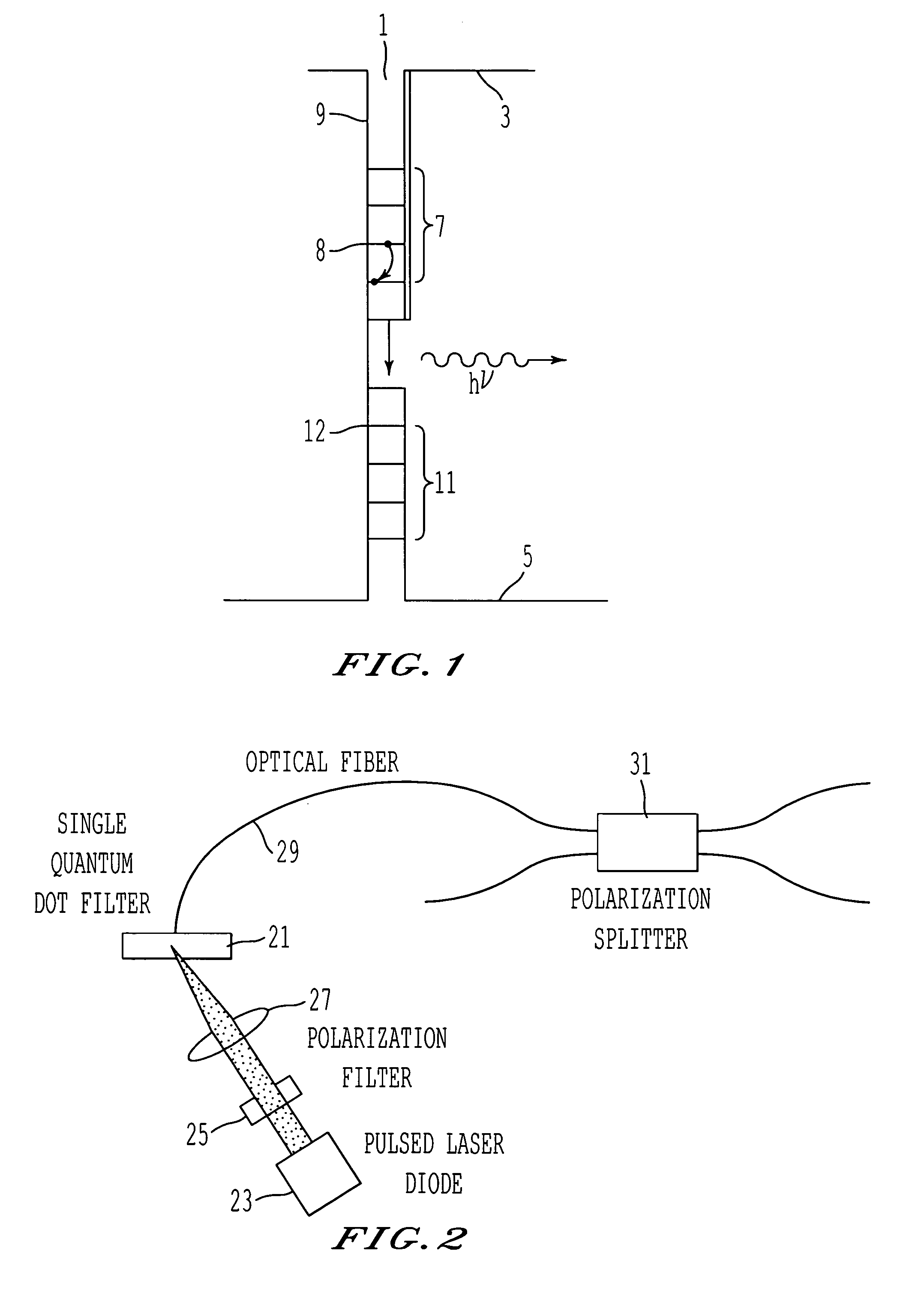
[0140]FIG. 1 shows a schematic band structure of a single quantum dot 1. The quantum dot forms a minimum in the conduction band 3 and a maximum in the valence band 5. A plurality of quantised conduction band levels 7 are formed in the minima 9 and a plurality of valence band levels 11 are formed in valence band maximum 13.

[0141]When a conduction band level 8 is populated by electron 15 and a valence band level 12 is populated by hole 17, the electron and hole recombine. Recombination of the single electron and a single hole results in the emission of a single photon.

[0142]The recombination of an electron and hole does not incur the instant that an electron and a hole populate the combined energy levels 7, 11. Instead, there is, on average, a finite delay between the population of the two levels and the emission of a photon. This is known as the “recombination time”. In a beam of conventional laser light, there are many photons. It is impossible using attenuation of a laser beam alon...


PUM


Abstract

A photon source comprising:a quantum dot (21) having a first confined energy level capable of being populated with an electron and a second confined energy level capable of being populated by a hole; andsupply means (23) for supplying carriers to the said energy levels, wherein the supply means are configured to supply a predetermined number of carriers to at least one of the energy levels to allow recombination of a predetermined number of carriers in said quantum dot to emit at least one photon.

Description

FIELD OF INVENTION[0001]The present invention relates to a photon source. More specifically, the present invention relates to a photon source which is capable of emitting single photons which are spaced apart by a predetermined time interval or pulses of n photons, where n is an integer can be controlled to the accuracy of a single photon.BACKGROUND OF INVENTION[0002]There is a need for such so-called single photon sources for use in optical quantum cryptography where, for example, the security key for an encryption algorithm is delivered by a stream of single photons which are regularly spaced in fine. It is essential for the security of this technique that each bit is encoded on just a single photon. This is because an eavesdropper tying to intercept the key will be forced to measure and thereby alter some photons during reading of the communication. Therefore, the intended recipient of the key can tell if the key has been intercepted.[0003]Such a source is also useful as a low-no...

Claims


Application Information

Patent Timeline
Patent Type & Authority Patents(United States)
IPC IPC(8): H01L29/225
CPCB82Y10/00B82Y20/00H01S5/3412H01S5/0078H01S5/02284Y10S977/95H01S5/06203H01S5/1042H01S5/18394H01S5/028H01S5/02251
Inventor SHIELDS, ANDREW J.HOGG, RICHARD A.
Owner KK TOSHIBA
Why Eureka
Try Eureka