

Chip level clock tree deskew circuit
a deskew circuit and clock signal technology, applied in the field of real-time, chip-level clock signal deskew circuits, can solve the problems of introducing delay into the clock signal net, natural skewed clock signals at different levels in the clock tree, and slight out of phas
- Summary
- Abstract
- Description
- Claims
- Application Information
AI Technical Summary
Benefits of technology
Problems solved by technology
Method used
Image

Examples
Embodiment Construction
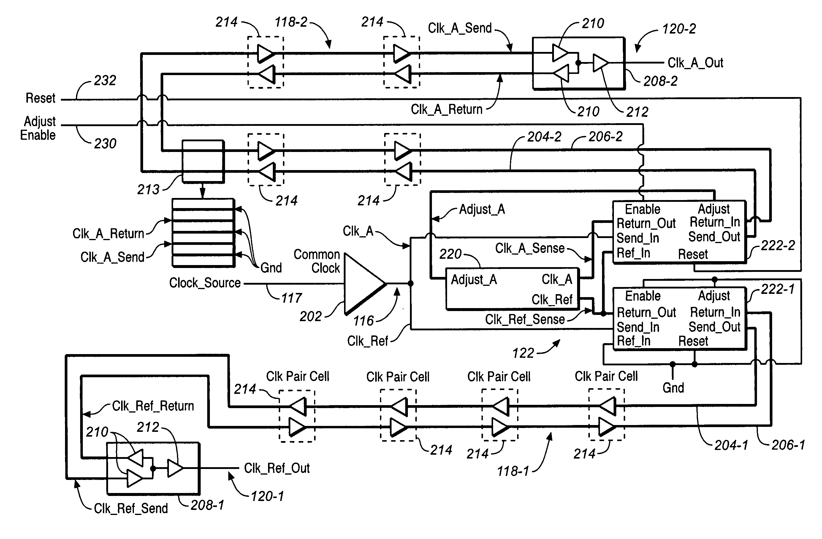
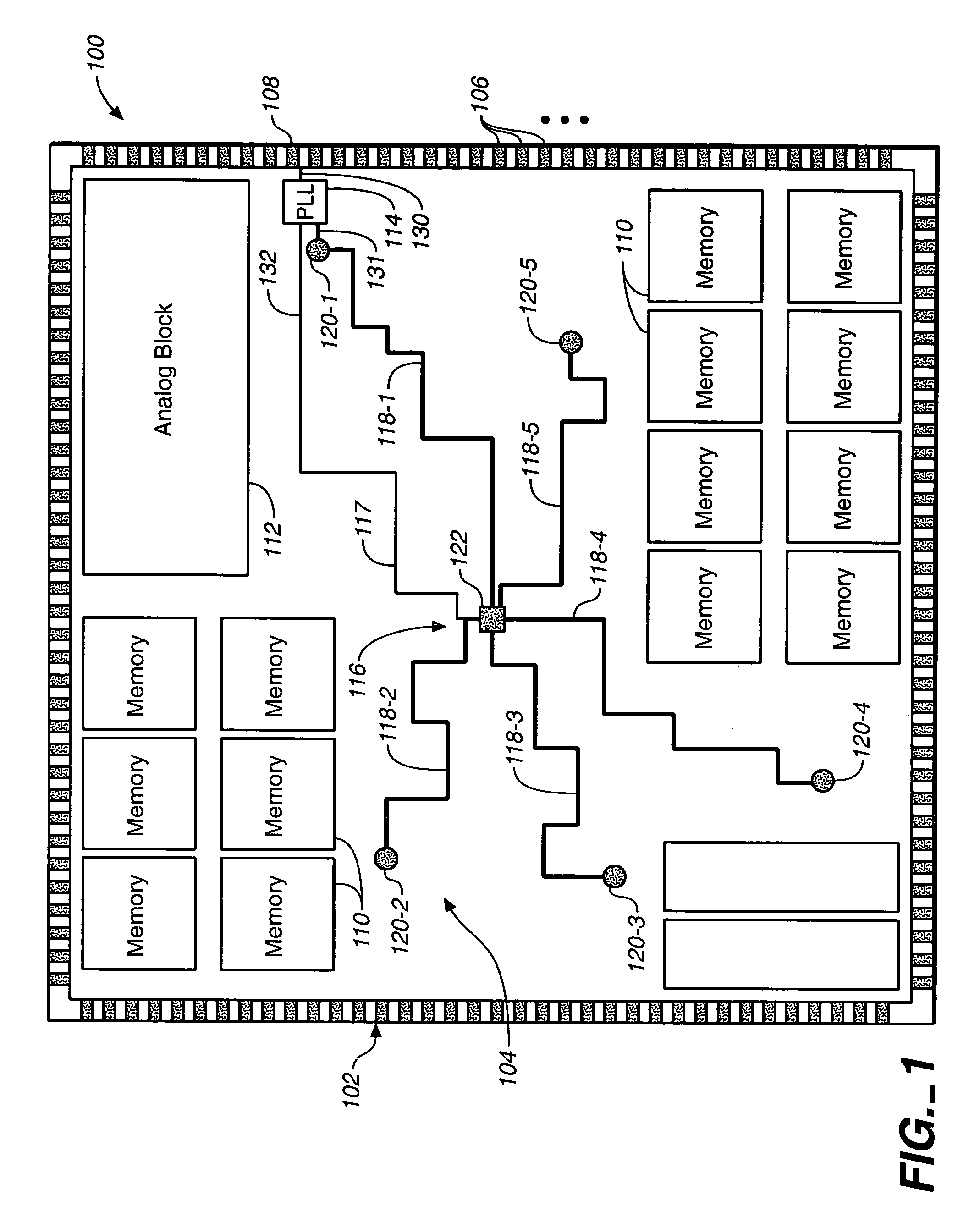
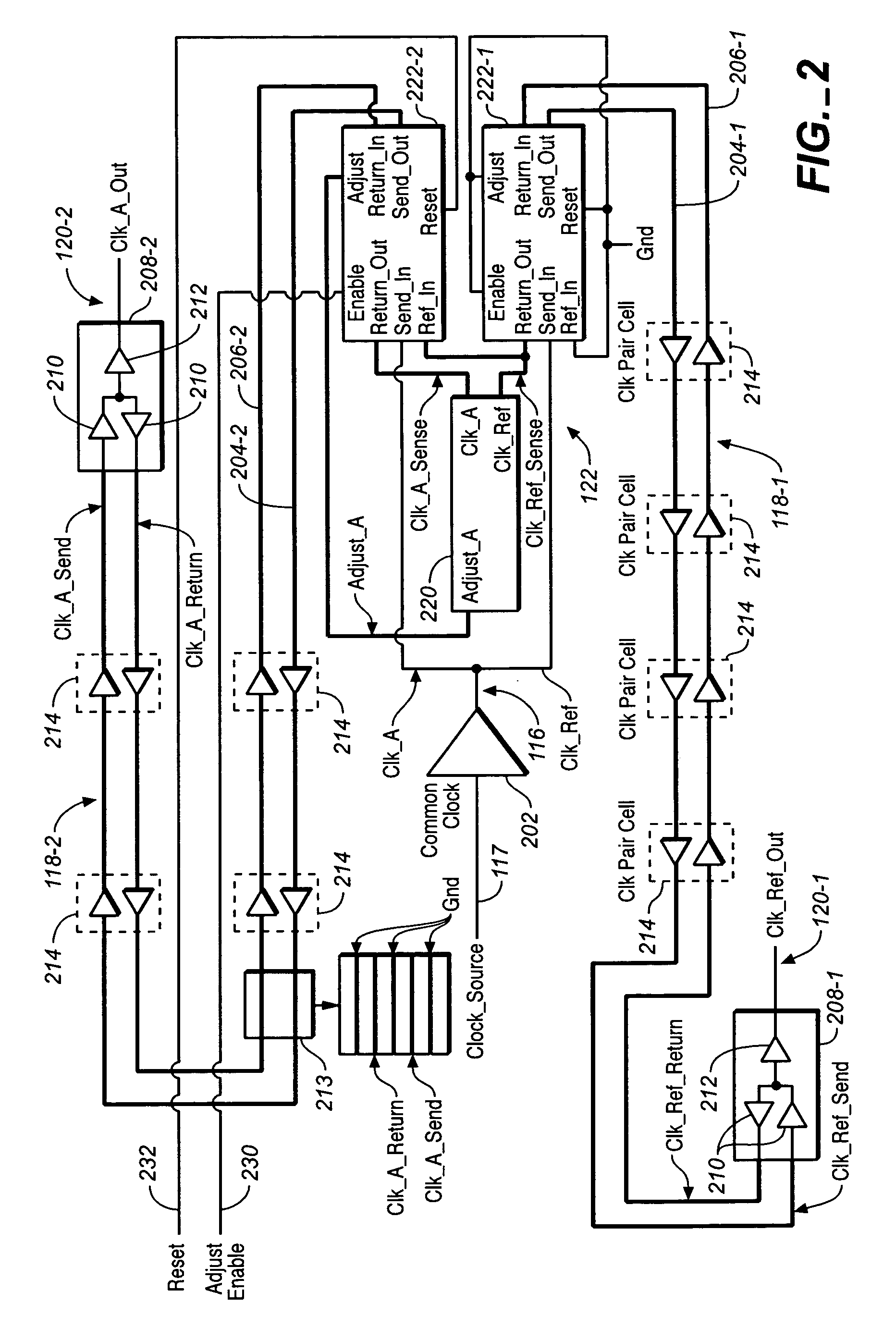
[0020]FIG. 1 is a diagram, which schematically illustrates a layout of an integrated circuit 100 according to one embodiment of the present invention. Integrated circuit 100 includes an input-output (I / O) region 102 and a core region 104. In this embodiment, I / O region 102 extends along the periphery of integrated circuit 100 and surrounds core region 104. However, I / O region 102 can be located in or along other areas of integrated circuit 100 or can be dispersed over a number of different areas in alternative embodiments of the present invention.
[0021]I / O region 102 includes I / O pads 106 for passing signals between core region 104 and devices that are external to integrated circuit 100. For example, I / O pads 106 can include a clock input 108 for receiving an external clock signal.
[0022]Core region 104 includes a plurality of semiconductor devices for implementing a desired function. In this example, core region 104 includes a plurality of embedded memory devices 110, an analog bloc...
PUM
 Abstract
Description
Claims
Application Information