High-speed synchronous memory device

a synchronous memory and high-speed technology, applied in the direction of information storage, static storage, digital storage, etc., can solve the problems of corresponding shortening, possible read errors, and insufficient equalization, and achieve the effect of not shortening the write driving tim

Inactive Publication Date: 2006-04-04
LAPIS SEMICON CO LTD
View PDF4 Cites 5 Cited by
  • Summary
  • Abstract
  • Description
  • Claims
  • Application Information

AI Technical Summary

Benefits of technology

[0014]A more specific object is to optimize the equalization time of the read data bus in a synchronous semiconductor memory device without shortening the driving time of the write data bus.
[0018]By generating the column control clock signal in different ways during read operations and write operations, the invention enables the equalization times of the read data bus and the write data bus to be separately optimized, so that the equalization time of the read data bus can be lengthened without lengthening the equalization time of the write data bus, thus without shortening the write driving time. The result is that the memory is able to operate at higher clock frequencies than if the column control clock signal were to be generated in the same way during both read and write operations.

Problems solved by technology

If this pulse width is comparatively short, as shown in FIG. 3, then at high clock frequencies, equalization may become inadequate, leading to possible read errors.
If the pulse width of the column control clock signal 510 is lengthened, however, then the interval during which the write driver 38 is activated may is correspondingly shortened, leading to possible write errors.

Method used


Image

  • High-speed synchronous memory device
  • High-speed synchronous memory device
  • High-speed synchronous memory device

Examples


Embodiment Construction

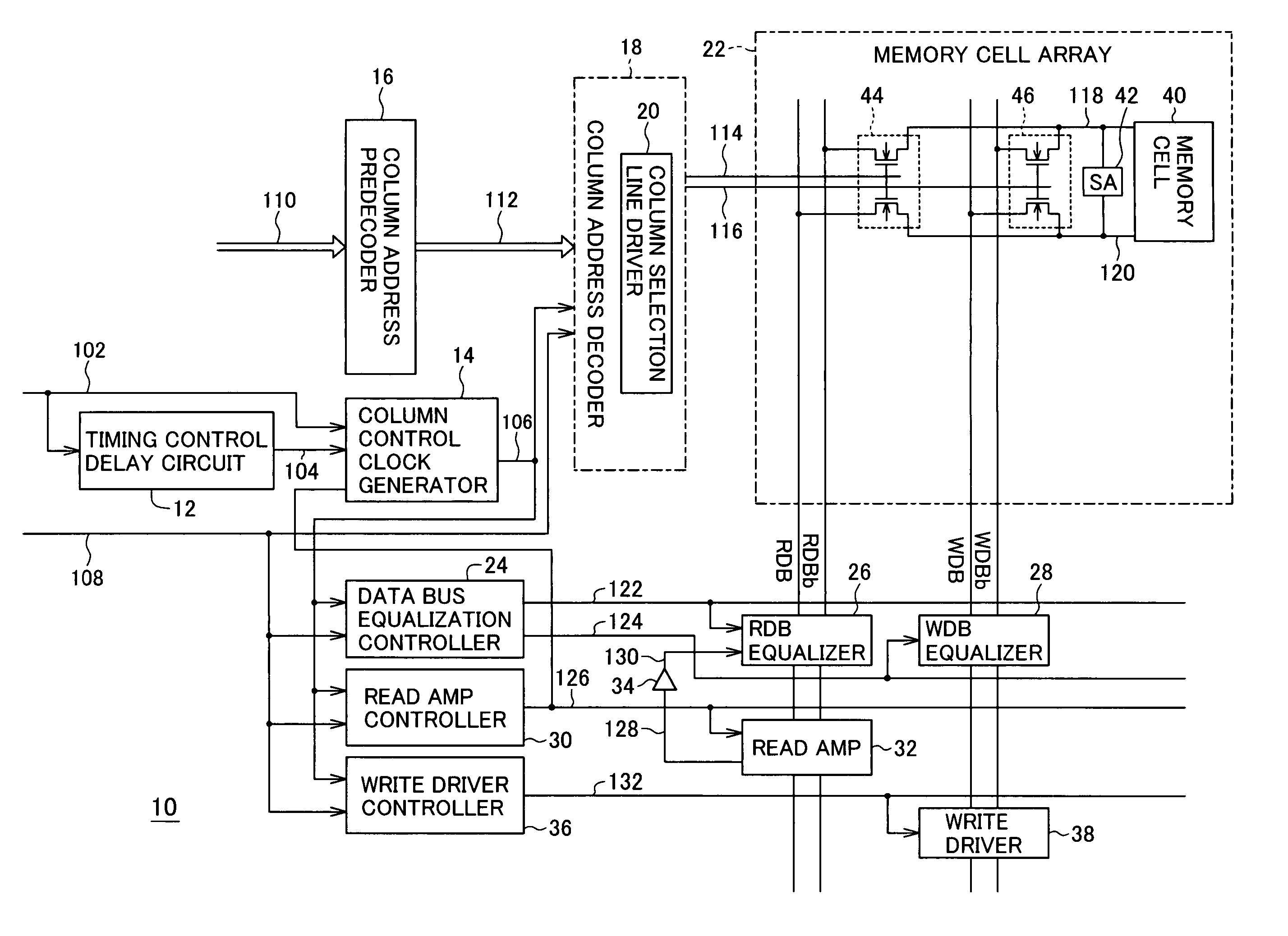
[0029]A synchronous semiconductor memory device embodying the invention will now be described with reference to the attached drawings, in which like elements are indicated by like reference characters. Elements not relevant to the invention are omitted from the drawings. Signals and the signal lines on which they are carried will be identified by the same reference numerals.

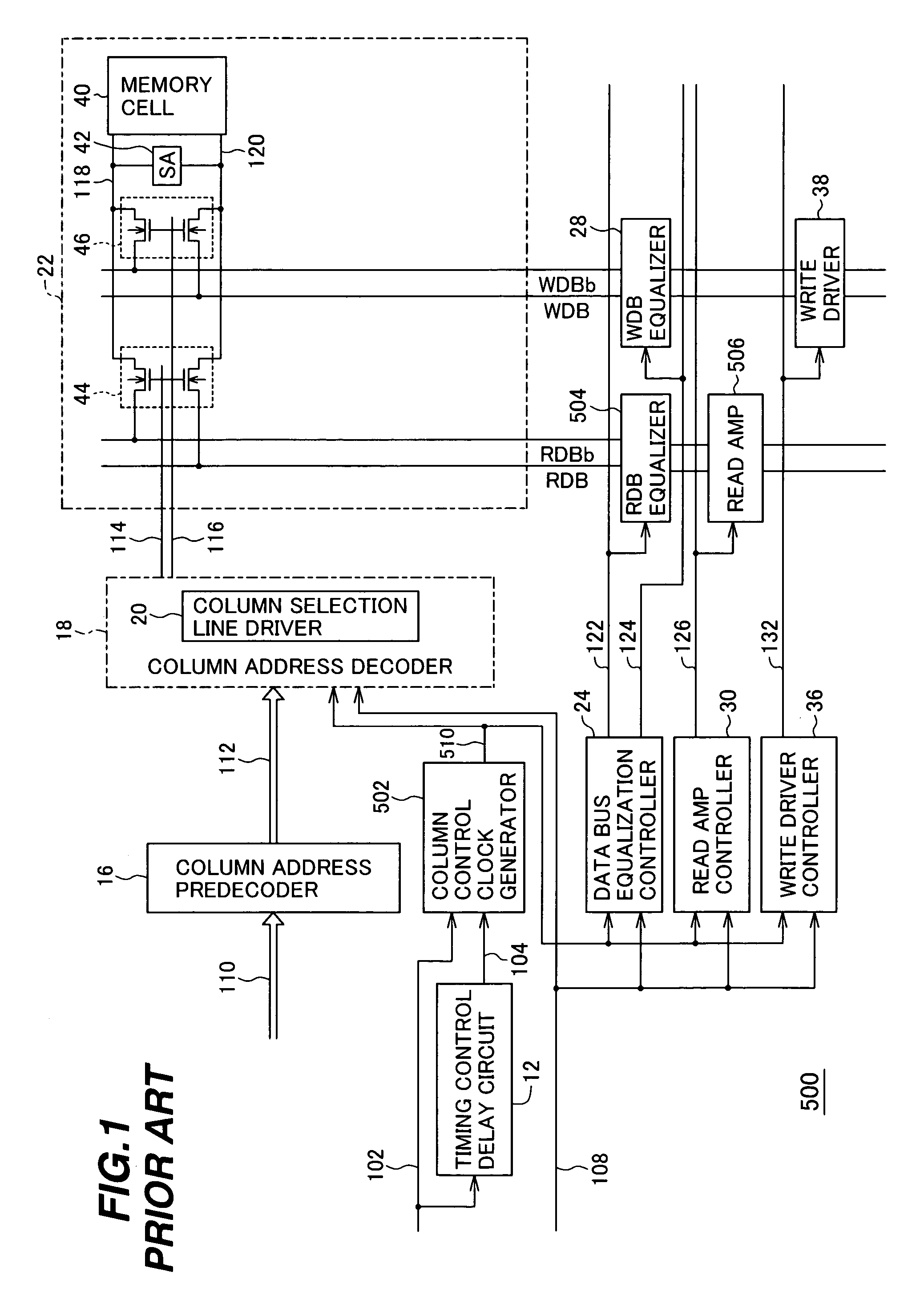
[0030]Referring to FIG. 4, like the conventional synchronous semiconductor memory device 500, the invented synchronous semiconductor memory device 10 operates in accordance with a clock signal 102, a read signal 108, and a column address signal 110. The clock signal 102 is supplied from an external source, and is used to synchronize all operations of the synchronous semiconductor memory device 10. The read signal 108, which is high during read operations and low during write operations, is typically generated from external command input signals. The column address signal 110 is generated from an external address ...


PUM


Abstract

A synchronous semiconductor memory device has a read data bus for transferring data from a memory cell array to a read amplifier, and a write data bus for transferring data from a write driver to the memory cell array. To control equalization of the read and write data buses, an internal control clock signal is driven to a first level in delayed synchronization with an external clock signal, to a second level in synchronization with the external clock signal at the end of write operations, and to the second level in synchronization with a read amplifier control signal during read operations. The read and write data bus equalization times can therefore be separately optimized, enabling the memory to operate at a higher clock frequency than if the internal control clock signal were to be generated in the same way during both read and write operations.

Description

BACKGROUND OF THE INVENTION[0001]1. Field of the Invention[0002]The present invention relates to a synchronous semiconductor memory device capable of operating at a high clock frequency, such as a high-speed synchronous dynamic random access memory (SDRAM).[0003]2. Description of the Related Art[0004]In the reading of data from a memory cell in a high-frequency synchronous semiconductor memory device, and in the writing of data into the memory cell, the data must be reliably transmitted over data transmission lines having a large line capacitance. In particular, when the data transmission lines swing the full distance between the power supply potential (the high logic level) and the ground potential (the low logic level), read access must be preceded by an adequate equalization time.[0005]To enable an adequate equalization time to be obtained at a high clock frequency, Japanese Unexamined Patent Application Publication No. 2001-155485 inserts selector switching elements between the ...

Claims


Application Information

Patent Timeline
Patent Type & Authority Patents(United States)
IPC IPC(8): G11C7/00G11C11/401G11C7/08G11C7/10G11C8/00G11C8/18G11C11/403
CPCG11C7/08G11C8/18G11C7/1072G11C7/1048
Inventor MIZUHASHI, HIROSHI
Owner LAPIS SEMICON CO LTD
Why Eureka
Try Eureka