Semiconductor device with surge protection circuit capable of preventing current leakage

a technology of surge protection circuit and semiconductor device, which is applied in the direction of semiconductor device details, semiconductor/solid-state device details, diodes, etc., can solve the problems of surge protection circuit not operating normally, and the pn junction expansion of the pn junction to increase the breakdown voltage of the diod

Inactive Publication Date: 2006-04-11
RENESAS ELECTRONICS CORP
View PDF7 Cites 15 Cited by
  • Summary
  • Abstract
  • Description
  • Claims
  • Application Information

AI Technical Summary

Benefits of technology

[0013]An object of the present invention is to provide a semiconductor device having a surge protection circuit without suffering from occurrence of current leakage and thus operating normally.
[0015]In the semiconductor device of the present invention, the first cathode region electrically connected to the first conductive layer and the second cathode region constituting the pn junction where Zener breakdown occurs are separately formed. Therefore, the impurity concentration of the first cathode region can be increased to reduce contact resistance with the first conductive layer. Moreover, the impurity concentrations of the anode region and the second cathode region can be reduced to prevent current leakage. Further, as the pn junction between the anode region and the second cathode region where Zener breakdown occurs is distant from the field oxide film, a problem that the breakdown voltage of the diode increases can be solved. Here, the increase of the breakdown voltage is caused when electrons that are present in the depletion layer of the pn junction between the anode region and the cathode region are trapped in the field oxide film to expand the depletion layer of the pn junction. Accordingly, the semiconductor device having the surge protection circuit without suffering from current leakage and thus operating normally can be achieved.

Problems solved by technology

Then, a problem arises that the depletion layer of the pn junction expands to increase the breakdown voltage of the diode.
A phenomenon (leakage of current) then occurs that is current flow in the surge protection circuit with any voltage lower than the breakdown voltage, resulting in a problem that the surge protection circuit does not operate normally.

Method used


Image

  • Semiconductor device with surge protection circuit capable of preventing current leakage
  • Semiconductor device with surge protection circuit capable of preventing current leakage
  • Semiconductor device with surge protection circuit capable of preventing current leakage

Examples


first embodiment

[0045

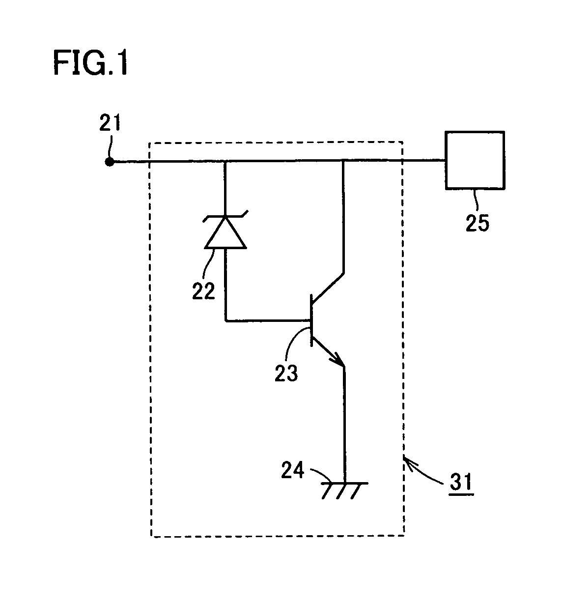
[0046]Referring to FIG. 1, a surge protection circuit 31 includes a diode 22 and an npn transistor 23. The cathode of diode 22 and the collector of npn transistor 23 are electrically connected to a signal input terminal 21 and to a device portion 25. The anode of diode 22 and the base of npn transistor 23 are electrically connected to each other. The emitter of npn transistor 23 is electrically connected to a ground potential 24.

[0047]A configuration of a semiconductor device having the surge protection circuit in this embodiment is now described.

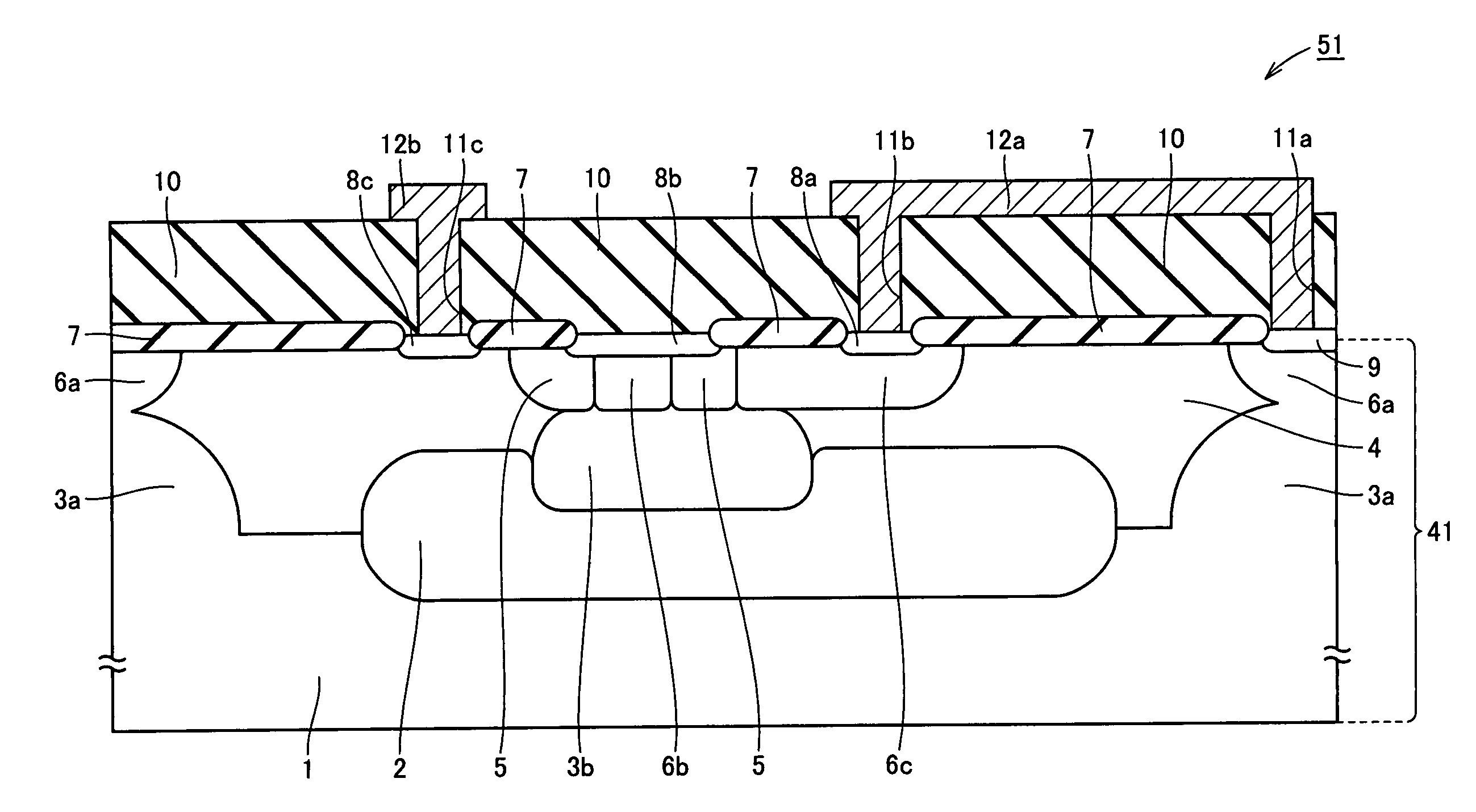
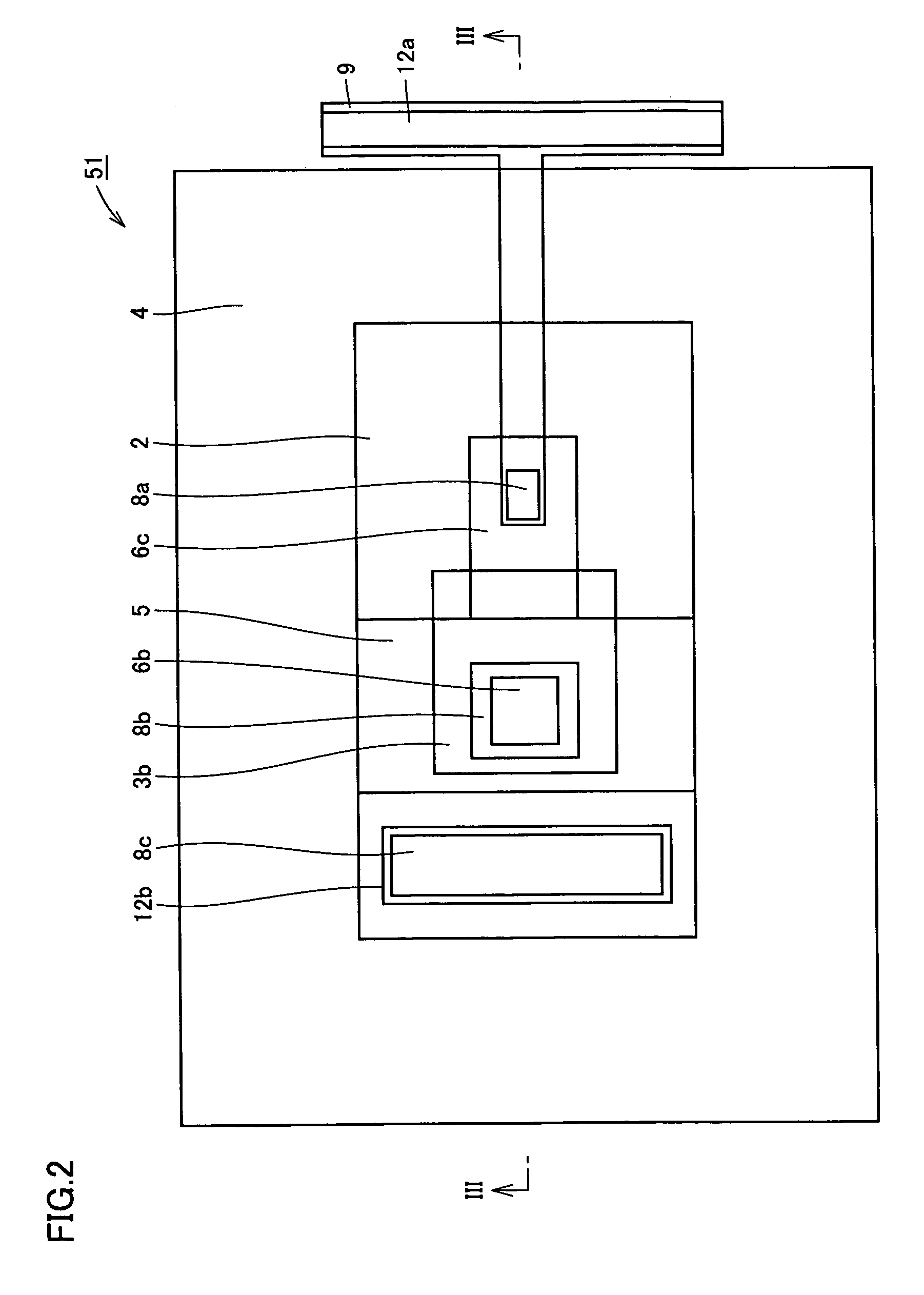
[0048]Referring to FIGS. 2 and 3, a semiconductor device 51 has a p− region 1 formed in a lower part of a semiconductor substrate 41 formed, for example, of silicon single crystal. On p− region 1, an n+ diffusion layer 2 is formed by implantation and diffusion. On this n+ diffusion layer 2, an n− epitaxial layer 4 is formed. On p− region 1, a p+ diffusion layer 3a and a p-type diffusion layer 6a are formed to enclose n− epitaxial layer...

second embodiment

[0066

[0067]Referring to FIGS. 5 and 6, according to this embodiment, an n+ diffusion layer 13a is formed in n− epitaxial layer 4 to enclose n+ diffusion layer 8c. N+ diffusion layer 13a is formed by implantation and diffusion of, for example, phosphorus glass into n− epitaxial layer 4 so as to reach n+ diffusion layer 2. Then, the collector region of npn transistor 23 is constituted of n+ diffusion layer 8c, n+ diffusion layer 13a, n+ diffusion layer 2 and n− epitaxial layer 4. N+ diffusion layer 13a has its impurity concentration higher than that of n− epitaxial layer 4.

[0068]It is noted that the configuration here is almost similar to that of the first embodiment shown in FIGS. 1–3 except for the above-discussed details. The same components are thus denoted by the same reference character and description thereof is not repeated here.

[0069]In the semiconductor device having the surge protection circuit of this embodiment, the collector region of npn transistor 23 is constituted add...

third embodiment

[0072

[0073]Referring to FIG. 7, according to this embodiment, an n+ diffusion layer 13b is further formed in n− epitaxial layer 4 on the right side (in FIG. 7) of p-type diffusion layer 6a. N+ diffusion layer 13b is formed by a similar method to that for n+ diffusion layer 13a. Then, the collector region of npn transistor 23 is constituted of n+ diffusion layer 8c, n+ diffusion layer 13a, n+ diffusion layer 2, n+ diffusion layer 13b and n− epitaxial layer 4.

[0074]It is noted that the configuration here is almost similar to that of the second embodiment shown in FIG. 6 except for the above-discussed details. The same components are thus denoted by the same reference character and description thereof is not repeated here.

[0075]In the semiconductor device having the surge protection circuit of this embodiment, the collector region of npn transistor 23 is additionally constituted of n+ diffusion layer 13b. As the n+ diffusion layer has a higher impurity concentration than that of the n−...


PUM


Abstract

A semiconductor device has a surge protection circuit electrically connected to a signal input terminal and including a diode and a transistor. The diode has its cathode region constituted of an n+ diffusion layer, an n− epitaxial layer, an n-type diffusion layer and an n+ diffusion layer. The n+ diffusion layer is electrically connected to a conductive layer and formed at a main surface of a semiconductor substrate. The n+ diffusion layer constitutes, together with a p-type diffusion layer, a pn junction where Zener breakdown occurs, and the pn junction with the Zener breakdown occurring therein is distant from a field oxide film. Then, the semiconductor device with the surge protection circuit without suffering from current leakage and thus normally operating can be achieved.

Description

[0001]This application a continuation-in-part of application Ser. No. 10 / 657,106, filed Sep. 9, 2003, now abandoned.BACKGROUND OF THE INVENTION[0002]1. Field of the Invention[0003]The present invention relates to semiconductor devices and more particularly to a semiconductor device having a surge protection circuit.[0004]2. Description of the Background Art[0005]There have been proposed various surge protection circuits for protecting, a motor vehicle, a motor, a fluorescent display and an audio device, for example, as well as an IC (Integrated Circuit) constituted of transistor devices for example, from an instantaneously increased current or voltage (surge). One of the proposed circuits, a surge protection circuit constituted of one diode and one npn transistor is known as a device which can be implemented with a simple configuration. A conventional surge protection circuit constituted of one diode and one npn transistor is configured as detailed below.[0006]In the conventional su...

Claims


Application Information

Patent Timeline
Patent Type & Authority Patents(United States)
IPC IPC(8): H01L27/102H01L27/02H01L29/73
CPCH01L27/0255H01L29/7302H01L27/0266
Inventor YAMAMOTO, FUMITOSHIUENISHI, AKIO
Owner RENESAS ELECTRONICS CORP
Why Eureka
Try Eureka