
Organic EL display device

a display device and organic technology, applied in static indicating devices, solid-state devices, instruments, etc., can solve the problems of display devices having a disadvantage in the aperture rate of display, and achieve the effects of reducing the aperture rate, reducing the variation in luminance among pixels, and small sacrifice to the aperture ra

Inactive Publication Date: 2006-04-11
DAI NIPPON PRINTING CO LTD
View PDF6 Cites 15 Cited by
  • Summary
  • Abstract
  • Description
  • Claims
  • Application Information

AI Technical Summary

Benefits of technology

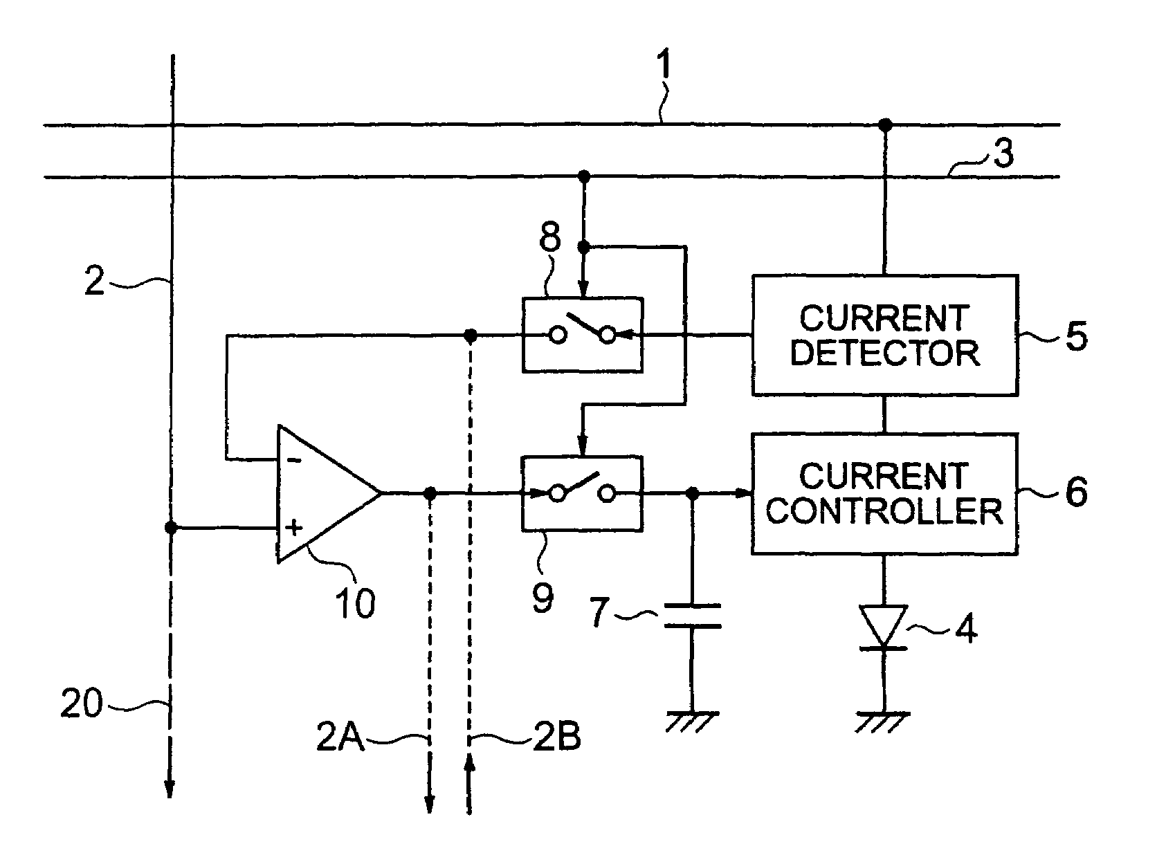
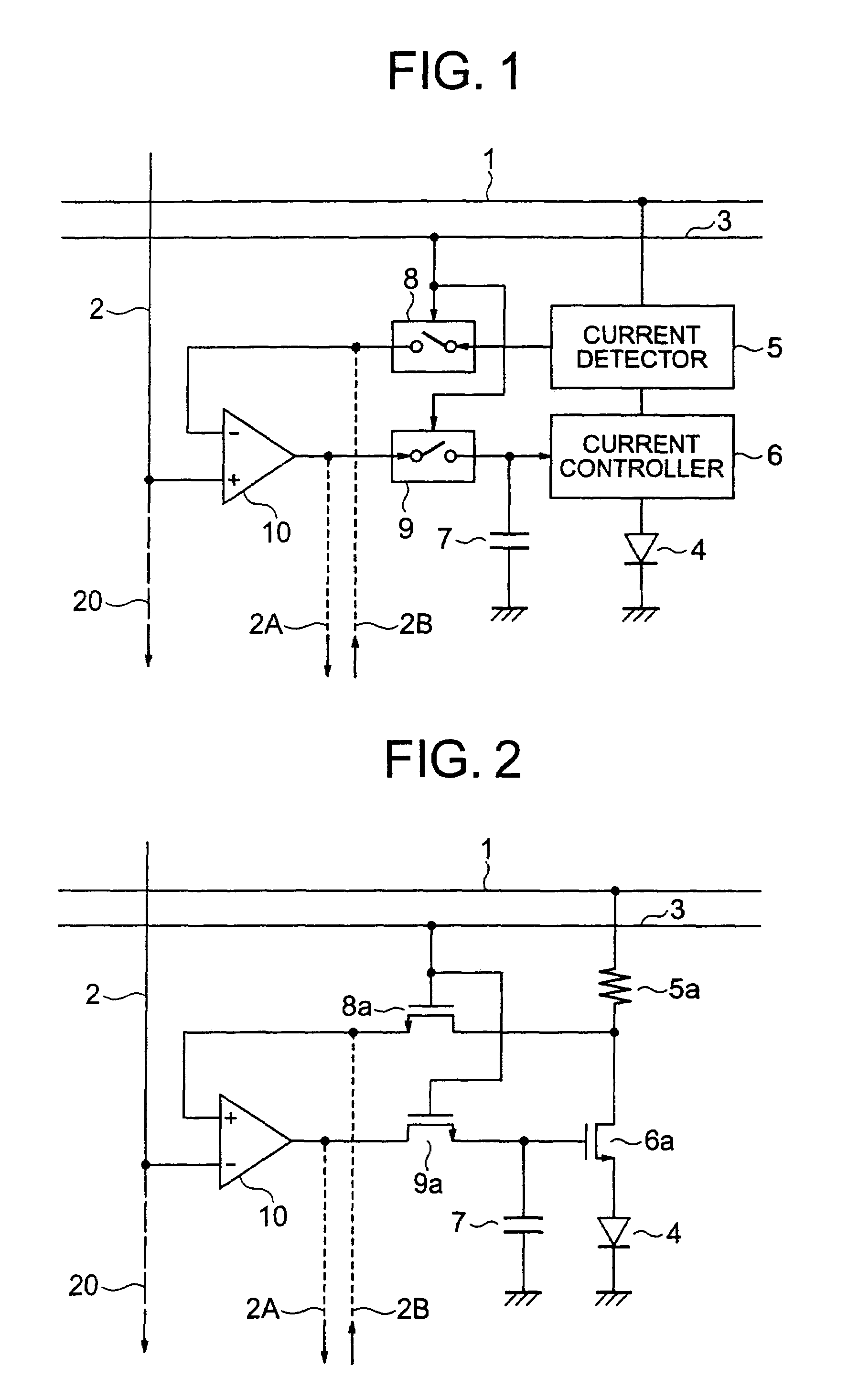
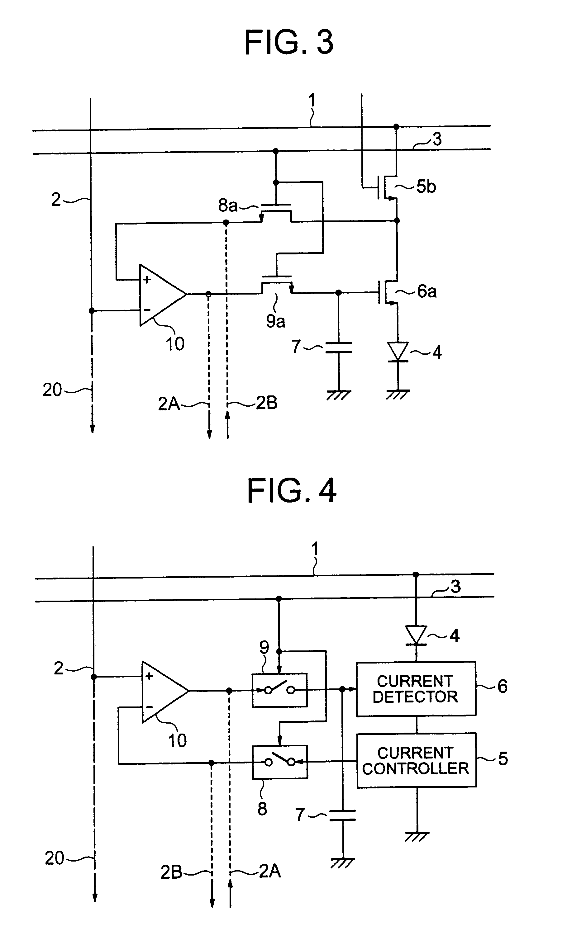
The present invention provides an organic EL display device using self-luminous organic EL elements as pixels, which are arranged in a matrix form to perform display. The device reduces variations in luminance among the pixels and minimizes sacrifice to the aperture rate. The device includes a light emitter, a current controller, a current detector, a first switching unit, a comparison amplifier, a second switching unit, and an image signal holding capacitor. The image signal is inputted into the comparison amplifier, and voltage is supplied to the current detector via the first switching unit. The output from the comparison amplifier is supplied to the image signal holding capacitor and the current controller via the second switching unit. The device uses the first switching unit in each pixel as a multiplexer and the second switching unit in each pixel as a demultiplexer. The device also includes negative feedback performed by the comparison amplifier to absorb variations in the input voltage versus output current characteristics of the current controllers and obtain current values that are identical among the pixels to a certain image signal. Overall, the device reduces variations in luminance among the pixels and minimizes sacrifice to the aperture rate.

Problems solved by technology

However, necessarily, an error amplifier circuit required for negative feedback needs to be built in for each pixel, and therefore it is considered that the display device has a disadvantage in the aperture rate of display (rate of net area of light emitter to surface area).

Method used


Image

  • Organic EL display device
  • Organic EL display device
  • Organic EL display device

Examples


Embodiment Construction

[0022]Embodiments of the present invention will be described with reference to the drawings which are not intended to limit the invention by any means but are provided only for the purpose of illustration.

[0023]As a form of an embodiment of the present invention, the aforementioned current detector can be a resistor inserted and connected between a power supply and the aforementioned current controller, and the aforementioned light emitter can be inserted and connected between the current controller and ground. This configuration employs as the current detector the resistor having a simple configuration and the light emitter formed based on ground.

[0024]Here, the current detector may detect the value of current flowing through the light emitter as voltage through use of the on-state resistance of a thin film transistor inserted and connected between the power supply and the current controller. This avoids the necessity for building in the resistor, bringing about advantages over man...


PUM


Abstract

Disclosed is an organic EL display device which includes a light emitter; a current controller controlling a current to be fed to the light emitter; a current detector detecting a value of current flowing through the light emitter as a voltage; a first switching unit switching between transmission and non-transmission of a voltage value corresponding to the detected current; a comparison amplifier comparing and amplifying the voltage value transmitted from the first switching unit to a voltage value corresponding to the image signal; a second switching unit switching between transmission and non-transmission of the voltage value being a result of the comparison and amplification; and an image signal holding capacitor charged / discharged based on the voltage value transmitted from the second switching unit, the current controller controlling the current to be fed to the light emitter based on a charging voltage of the image signal holding capacitor.

Description

BACKGROUND[0001]1. Field of the Invention[0002]The present invention relates to an organic EL display device which performs display using self-luminous EL (electroluminescence) elements as pixels which are arranged in a matrix form and, more specifically, to an organic EL display device suitable for reducing variations in luminance among pixels.[0003]2. Description of the Related Art[0004]Display devices employing organic EL elements have characteristics, not realized by LCDs (liquid crystal display devices), in that the organic EL elements require no backlights because they are self-luminous elements and thus suitable for reducing power consumption. Those display devices further have fast response and wide viewing angle characteristics, and also have advantages that they are adaptable to flexible applications and so on since the elements themselves are solid.[0005]Possible systems of driving the organic EL display device include, similarly to LCD, PM (passive matrix) drive and AM (...

Claims


Application Information

Patent Timeline
Patent Type & Authority Patents(United States)
IPC IPC(8): G09G3/32G09G3/20H01L51/50G09G3/30
CPCG09G3/3233G09G3/3291G09G2320/0233G09G2300/0847G09G2300/0809
Inventor SATO, YASUSHIHIGUCHI, TAKUYA
Owner DAI NIPPON PRINTING CO LTD
Learn More