Carrier and clock recovery using universal frequency translation

Inactive Publication Date: 2006-04-11
PARKER VISION INC
649 Cites 75 Cited by

AI-Extracted Technical Summary

Problems solved by technology

Conventional coherent detection systems suffer from the disadvantage of being relatively expensive in terms of cost and power consumption.
Conventional wireless communications circuitry is complex and has a large numbe...

Method used

[0159]FIG. 20A illustrates an aliasing module 2000 for down-conversion using a universal frequency translation (UFT) module 2002 which down-converts an EM input signal 2004. In particular embodiments, aliasing module 2000 includes a switch 2008 and a capacitor 2010. The electronic alignment of the circuit components is flexible. That is, in one implementation, the switch 2008 is in series with input signal 2004 and capacitor 2010 is shunted to ground (although it may be other than ground in configurations such as differential mode). In a second implementation (see FIG. 20G), the capacitor 2010 is in series with the input signal 2004 and the switch 2008 is shunted to ground (although it may be other than ground in configurations such as differential mode). Aliasing module 2000 with UFT module 2002 can be easily tailored to down-convert a wide variety of electromagnetic signals using aliasing frequencies that are well below the frequencies of the EM input signal 2004.
[0196]One of the steps in determining the characteristic input impedance of the energy transfer module could be to measure its value. In an embodiment, the energy transfer module's characteristic input impedance is 300 ohms. An impedance matching circuit can be utilized to efficiently couple an input EM signal that has a source impedance of, for example, 50 ohms, with the energy transfer module's impedance of, for example, 300 ohms. Matching these impedances can be accomplished in various manners, including providing the necessary impedance directly or the use of an impedance match circuit as described below.
[0199]In an embodiment, the energy transfer module's characteristic output impedance is 2K ohms. An impedance matching circuit can be utilized to efficiently couple the down-converted signal with an output impedance of, for example, 2K ohms, to a load of, for example, 50 ohms. Matching these impedances can be accomplished in various manners, including providing the necessary load impedance directly or the use of an impedance match circuit as described below.
[0204]Resonant tank and other resonant structures can be used to further optimize the energy transfer characteristics of the invention. For example, resonant structures, resonant about the input frequency, can be used to store energy from the input signal when the switch is open, a period during which one may conclude that the architecture would otherwise be limited in its maximum possible efficiency. Resonant tank and other resonant structures can include, but are not limited to, surface acoustic wave (SAW) filters, dielectric resonators, diplexers, capacitors, inductors, etc.
[0212]An energy transfer signal 6042 controls a switch 6014. When the energy transfer signal 6042 controls the switch 6014 to open and close, high frequency signal components are not allowed to pass through tank1 or tank2. However, the lower signal components (50 Mhz in this embodiment) generated by the system are allowed to pass through tank1 and tank2 with little attenuation. The effect of tank1 and tank2 is to further separate the input and output signals from the same node thereby producing a more stable input and output impedance. Capacitors 6018 and 6040 act to store the 50 MHZ output signal energy between energy transfer pulses.
[0213]Further energy transfer optimization is provided by placing an inductor 6010 in series with a storage capacitor 6012 as shown. In the illustrated example, the series resonant frequency of this circuit arrangement is approximately 1 GHz. This circuit increases the energy transfer characteristic of the system. The ratio of the impedance of inductor 6010 and the impedance of the storage capacitor 6012 is preferably kept relatively small so that the majority of the energy available will be transferred to storage capacitor 6012 during operation. Exemplary output signals A and B are illustrated in FIGS. 60B and 60C, respectively.
[0215]FIG. 55 illustrates a shunt tank circuit 5510 in a single-ended to-single-ended system 5512. Similarly, FIG. 63 illustrates a shunt tank circuit 6310 in a system 6312. The tank circuits 5510 and 6310 lower driving source impedance, which improves transient response. The tank circuits 5510 and 6310 are able store the energy from the input signal and provide a low driving source impedance to transfer that energy throughout the aperture of the closed switch. The transient nature of the switch aperture can be viewed as having a response that, in addition to including the input frequenc...

Benefits of technology

[0026]An advantage of the present invention is that is enables a coherent receiver circuit to be fabricated on a single semiconductor substrate. In other words, the UFT module allows the phase locked loop to be configured as an analog circuit that is on-chip with the analog down-conversion and up-conversion circuitry. This configuration uses less power than a DSP phase lock loop solution, as analog solutions are almo...

Abstract

Coherent detection of a received EM signal using universal frequency translation (UFT) is described herein. The received EM signal is sampled according to a sub-harmonic LO signal, where the LO signal is in frequency and phase coherence with the received EM signal. The coherent receiver includes a down-converter/demodulator and a synthesizer/loop filter that are both implemented using UFT technology. The down-converter/demodulator samples the EM input signal using a UFT module according to the coherent sub-harmonic LO signal that is generated by the synthesizer/loop filter. The synthesizer/loop filter generates the coherent LO signal using a phase detector, a loop filter, and an up-converter. The phase detector and up-converter are implemented using UFT modules.

Application Domain

Technology Topic

Image

  • Carrier and clock recovery using universal frequency translation
  • Carrier and clock recovery using universal frequency translation
  • Carrier and clock recovery using universal frequency translation

Examples

  • Experimental program(1)

Example

7. Example Application Embodiments of the Invention
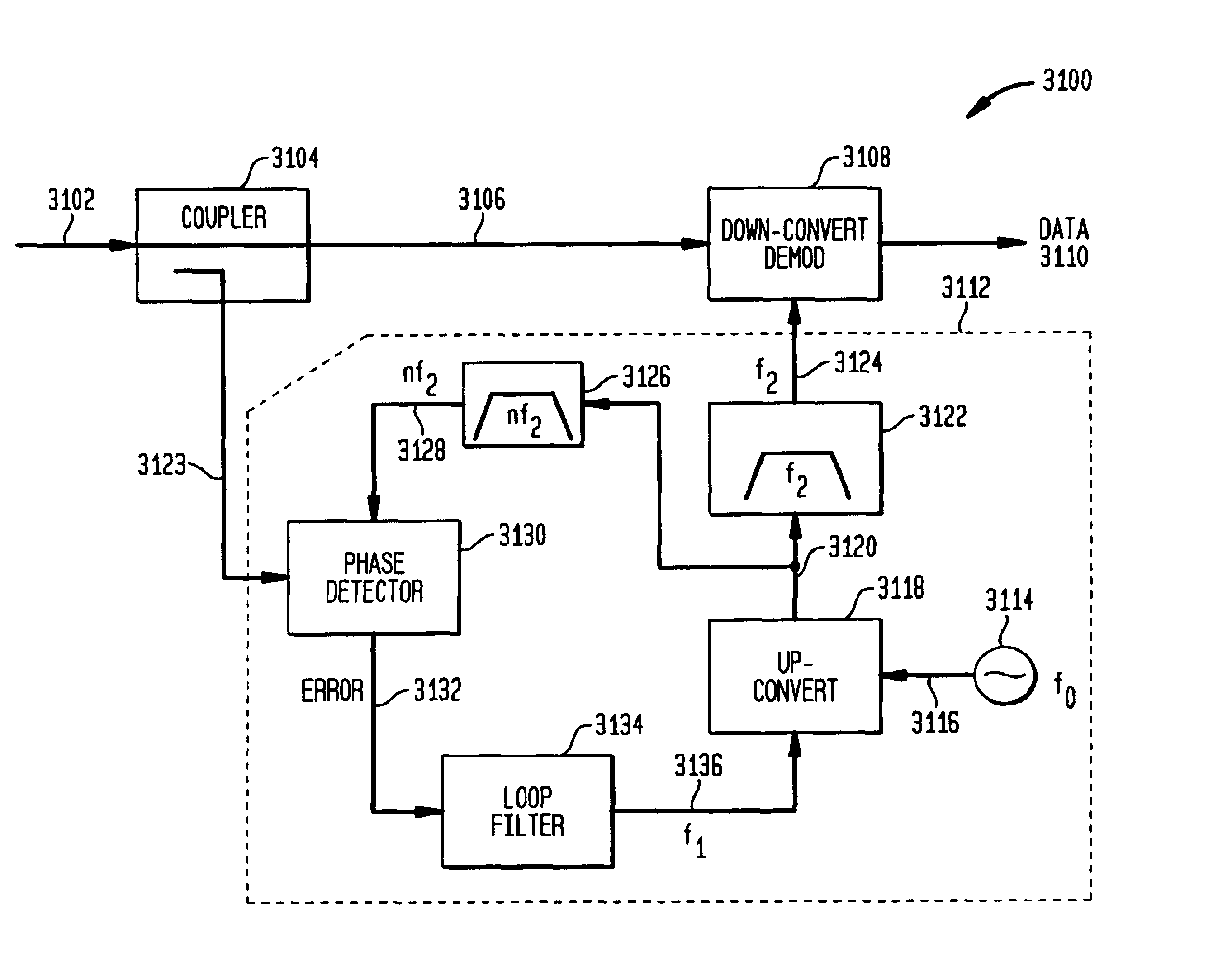
[0358]As noted above, the UFT module of the present invention is a very powerful and flexible device. Its flexibility is illustrated, in part, by the wide range of applications in which it can be used. Its power is illustrated, in part, by the usefulness and performance of such applications.
[0359]Example applications of the UFT module were described above. In particular, frequency down-conversion, frequency up-conversion, enhanced signal reception, and unified down-conversion and filtering applications of the UFT module were summarized above, and are further described below. These applications of the UFT in module are discussed herein for illustrative purposes. The invention is not limited to these example applications. Additional applications of the UFT module will be apparent to persons skilled in the relevant art(s), based on the teachings contained herein.
[0360]For example, the present invention can be used in applications that involve frequency down-conversion. This is shown in FIG. 1C, for example, where an example UFT module 115 is used in a down-conversion module 114. In this capacity, the UFT module 115 frequency down-converts an input signal to an output signal. This is also shown in FIG. 7, for example, where an example UFT module 706 is part of a down-conversion module 704, which is part of a receiver 102.
[0361]The present invention can be used in applications that involve frequency up-conversion. This is shown in FIG. 1D, for example, where an example UFT module 117 is used in a frequency up-conversion module 116. In this capacity, the UFT module 117 frequency up-converts an input signal to an output signal. This is also shown in FIG. 8, for example, where an example UFT module 806 is part of up-conversion module 804, which is part of a transmitter 802.
[0362]The present invention can be used in environments having one or more transmitters 902 and one or more receivers 906, as illustrated in FIG. 9. In such environments, one or more of the transmitters 902 may be implemented using a UFT module, as shown for example in FIG. 8. Also, one or more of the receivers 906 may be implemented using a UFT module, as shown for example in FIG. 7.
[0363]The invention can be used to implement a transceiver. An example transceiver 1002 is illustrated in FIG. 10. The transceiver 1002 includes a transmitter 1004 and a receiver 1008. Either the transmitter 1004 or the receiver 1008 can be implemented using a UFT module. Alternatively, the transmitter 1004 can be implemented using a UFT module 1006, and the receiver 1008 can be implemented using a UFT module 11010. This embodiment is shown in FIG. 10.
[0364]Another transceiver embodiment according to the invention is shown in FIG. 11. In this transceiver 1102, the transmitter 1104 and the receiver 1108 are implemented using a single UFT module 1106. In other words, the transmitter 1104 and the receiver 1108 share a UFT module 1106.
[0365]As described elsewhere in this application, the invention is directed to methods and systems for enhanced signal reception (ESR). Various ESR embodiments include an ESR module (transmit) in a transmitter 1202, and an ESR module (receive) in a receiver 1210. An example ESR embodiment configured in this manner is illustrated in FIG. 12.
[0366]The ESR module (transmit) 1204 includes a frequency up-conversion module 1206. Some embodiments of this frequency up-conversion module 1206 may be implemented using a UFT module, such as that shown in FIG. 1D.
[0367]The ESR module (receive) 1212 includes a frequency down-conversion module 1214. Some embodiments of this frequency down-conversion module 1214 may be implemented using a UFT module, such as that shown in FIG. 1C.
[0368]As described elsewhere in this application, the invention is directed to methods and systems for unified down-conversion and filtering (UDF). An example unified down-conversion and filtering module 1302 is illustrated in FIG. 13. The unified down-conversion and filtering module 1302 includes a frequency down-conversion module 1304 and a filtering module 1306. According to the invention, the frequency down-conversion module 1304 and the filtering module 1306 are implemented using a UFT module 1308, as indicated in FIG. 13.
[0369]Unified down-conversion and filtering according to the invention is useful in applications involving filtering and/or frequency down-conversion. This is depicted, for example, in FIGS. 15A-15F. FIGS. 15A-15C indicate that unified down-conversion and filtering according to the invention is useful in applications where filtering precedes, follows, or both precedes and follows frequency down-conversion. FIG. 15D indicates that a unified down-conversion and filtering module 1524 according to the invention can be utilized as a filter 1522 (i.e., where the extent of frequency down-conversion by the down-converter in the unified down-conversion and filtering module 1524 is minimized). FIG. 15E indicates that a unified down-conversion and filtering module 1528 according to the invention can be utilized as a down-converter 1526 (i.e., where the filter in the unified down-conversion and filtering module 1528 passes substantially all frequencies). FIG. 15F illustrates that the unified down-conversion and filtering module 1532 can be used as an amplifier. It is noted that one or more UDF modules can be used in applications that involve at least one or more of filtering, frequency translation, and amplification.
[0370]For example, receivers, which typically perform filtering, down-conversion, and filtering operations, can be implemented using one or more unified down-conversion and filtering modules. This is illustrated, for example, in FIG. 14.
[0371]The methods and systems of unified down-conversion and filtering of the invention have many other applications. For example, as discussed herein, the enhanced signal reception (ESR) module (receive) operates to down-convert a signal containing a plurality of spectrums. The ESR module (receive) also operates to isolate the spectrums in the down-converted signal, where such isolation is implemented via filtering in some embodiments. According to embodiments of the invention, the ESR module (receive) is implemented using one or more unified down-conversion and filtering (UDF) modules. This is illustrated, for example, in FIG. 16. In the example of FIG. 16, one or more of the UDF modules 1610, 1612, 1614 operates to down-convert a received signal. The UDF modules 1610, 1612, 1614 also operate to filter the down-converted signal so as to isolate the spectrum(s) contained therein. As noted above, the UDF modules 1610, 1612, 1614 are implemented using the universal frequency translation (UFT) modules of the invention.
[0372]The invention is not limited to the applications of the UFT module described above. For example, and without limitation, subsets of the applications (methods and/or structures) described herein (and others that would be apparent to persons skilled in the relevant art(s) based on the herein teachings) can be associated to form useful combinations.
[0373]For example, transmitters and receivers are two applications of the UFT module. FIG. 10 illustrates a transceiver 1002 that is formed by combining these two applications of the UFT module, i.e., by combining a transmitter 1004 with a receiver 1008.
[0374]Also, ESR (enhanced signal reception) and unified down-conversion and filtering are two other applications of the UFT module. FIG. 16 illustrates an example where ESR and unified down-conversion and filtering are combined to form a modified enhanced signal reception system.
[0375]The invention is not limited to the example applications of the UFT module discussed herein. Also, the invention is not limited to the example combinations of applications of the UFT module discussed herein. These examples were provided for illustrative purposes only, and are not limiting. Other applications and combinations of such applications will be apparent to persons skilled in the relevant art(s) based on the teachings contained herein. Such applications and combinations include, for example and without limitation, applications/combinations comprising and/or involving one or more of: (1) frequency translation; (2) frequency down-conversion; (3) frequency up-conversion; (4) receiving; (5) transmitting; (6) filtering; and/or (7) signal transmission and reception in environments containing potentially jamming signals.
[0376]Additional examples are set forth below describing applications of the UFT module in the area of coherent detection of a received electromagnetic signal.
8. Coherent Detection
[0377]FIG. 25 illustrates a direct down-conversion system 2500 for receiving an electromagnetic (EM) signal 2502 and directly down-converting the EM input signal 2502, to generate a data signal 2508. Down-converter system 2500 includes an antenna 2504, a down-converter 2506, and a sub-harmonic local oscillator (LO) 2510.
[0378]The antenna 2504 receives an electromagnetic signal 2502 having a carrier frequency fc, resulting in a received signal 2505. The received signal 2505 can be an unmodulated carrier signal, or can be modulated with data signal, as will be understood by those skilled in the arts.
[0379]The down-converter 2506 directly down-converts the received signal 2505 to the data signal 2508. In doing so, the down-converter 2506 samples the received signal 2505 according to an LO signal 2512, where the signal 2512 is generated by a local oscillator 2510. For direct down-conversion to baseband, the LO signal 2512 is preferably an exact sub-harmonic frequency of the carrier frequency fC. In other words, the LO signal 2512 is preferably frequency coherent with the received signal 2505. For down-conversion to an IF, the frequency of the LO signal is preferably the (fC+/−fIF)/n, where n represents a harmonic. Additionally, for optimal results, the LO signal 2512 is preferably phase coherent with the received signal 2505.
[0380]FIGS. 26-28 further illustrate the benefits of frequency coherence for the down-conversion system 2500 during direct down-conversion. FIG. 26 illustrates the signal 2505 as a modulated signal having a modulation spectrum, and also illustrates the LO signal 2512 as a pure tone. As shown in FIG. 27, if the frequency of the LO signal 2512 is exactly a sub-harmonic of fC, then the data signal 2508 is down-converted to baseband, as is desired. However, as shown in FIG. 27, if the LO signal 2512 is offset from an exact sub-harmonic frequency of the LO signal 2512 by a frequency delta 2802, then the data signal 2508 is offset from baseband by the frequency delta 2802. If the delta 2802 is large enough, then the data signal 2802 could fall outside of the filter passbands.
[0381]As illustrated above, frequency and phase coherence is often desirable for communications application. In practical communications systems, frequency and phase coherence can be difficult to achieve. This can occur because the operational tolerances of the LO 2510 can cause the LO signal 2512 to drift away from an exact sub-harmonic of fC. For example, temperature changes may cause either the LO signal 2512 drift in frequency over time so that the LO signal 2512 will not be an exact sub-harmonic of the EM input signal 2502. Similarly, the transmitter that generates the EM signal 2502 may drift from fC. Additionally, the EM signal 2502 may drift from fC due to transmission effects such as Doppler shift. Doppler shift occurs when the transmitter that generates the EM signal 2502 is moving during transmission, relative to the receiver 2500. In which case, the relative velocity of the transmitter manifests itself as a frequency shift in the EM signal 2502. Doppler is shift most notable in satellite communications, where the satellite may be moving at a significant velocity during earth orbit.
[0382]8.1 Universal Frequency Technology
[0383]As described herein and in related patents, universal frequency translation (UFT) can be utilized for down-converting an EM input signal to a lower frequency down-converted signal. This includes down-conversion to baseband or down-conversion to an IF.
[0384]FIG. 29 illustrates a down-converter 2900 that incorporates UFT technology. Down-converter 2900 includes a UFT module 2904, a storage module 2908, a pulse generator 2914, and a local oscillator 2918. The UFT module 2904 is configured as a controlled switch 2906. The down-converter 2900 receives an EM input signal 2902 at a frequency fC, and down-converts the EM input signal 2902 to a down-converted signal 2910. The down-converter 2900 operates as follows.
[0385]The oscillator 2918 generates a LO signal 2916 that is preferably a sub-harmonic of the input signal 2902. The LO signal 2916 is preferably a sinewave, however, other waveforms could be used including square waves, triangle waves, etc.
[0386]The pulse generator 2914 receives the LO signal 2916 and generates a control signal 2912. In embodiments, the control signal 2912 is a plurality of pulses having pulse widths (or apertures) that tend away from zero time. For example, and without limitation, the pulse widths can be approximately 1/10, ¼, ½, ¾, etc., or any other fraction of the period of the EM input signal 2902.
[0387]The UFT module 2904 receives the EM input signal 2902 and samples the EM input signal 2902 according to the control signal 2912. More specifically, the controlled switch 2906 samples the EM input signal 2902 according to the periodic control signal 2912, resulting in under-samples 2906. The pulse widths of the control signal 2912 transfer non-negligible amounts of energy from the EM input signal 2902 to the undersamples 2906. In embodiments, the controlled switch 2906 is implemented as a FET 3002, as shown in FIG. 30A. The control signal 2912 controls the gate of the FET 2912.
[0388]The storage module 2908 receives the undersamples 2906, and integrates the undersamples 2906, to generate the down-converted signal 2910. In embodiments, the storage module 2908 is a capacitor 3004 as shown in FIG. 30B, or an inductor 3006 as shown in FIG. 30C.
[0389]As in FIG. 26-28, the oscillator 2918 is preferably frequency coherent and phase coherent with the received EM input signal 2902. More specifically, the frequency of the LO signal 2916 is preferably an exact sub-harmonic of the EM input signal 2902.
[0390]8.2 Down-converter with Coherent Phase Lock Loop
[0391]FIG. 31 illustrates as receiver 3100 that can provide coherent direct down-conversion/demodulation of a received EM signal 3102 to generate a data signal 3110. In other words, the receiver 3100 can track frequency and phase changes in the EM signal 3102, so that sub-sampling during down-conversion is performed in frequency and phase coherence with the EM signal 3102. The receiver 3100 includes a coupler 3104, a direct down-converter/demodulator 3108, and a synthesizer/phase lock loop filter 3112. The synthesizer/loop filter generates a LO signal 3124 that used to directly down-convert and demodulate the EM signal 3102 in coherent manner. In other words, the signal 3124 is a coherent sub-harmonic of the EM signal 3102. The receiver 3100 is described in reference to the flowchart 3200, that is shown in FIG. 32.
[0392]In step 3202, the EM signal 3102 is received. The EM signal 3102 can be an unmodulated signal or a modulated signal as will be understood by those skilled in the relevant arts.
[0393]In step 3204, an in-phase coupler 3104 divides the signal 3102 to generate a direct signal 3106 and a coupled signal 3123. Both of the signals 3106 and 3123 are substantially similar to the signal 3102 in information and frequency content. However, preferably most of the signal power is transferred to the direct signal 3106, which is down-converted by the down-converter 3108. Whereas the coupled signal 3123 is used to generate a coherent sub-harmonic LO signal, which is used for down-conversion of the direct signal 3106.
[0394]In step 3206, the synthesizer/loop filter 3112 generates a coherent sub-harmonic LO signal 3124 from the coupled signal 3123. The LO signal 3124 has a frequency f2 that is substantially an exact sub-harmonic of the EM signal 3102, and is in phase coherence with the EM signal 3102. Therefore, if EM signal 3102 changes in frequency or phase, the LO signal 3124 varies in frequency and/or phase to track changes in the EM signal 3102.
[0395]In step 3208, the down-converter/demodulator 3108 directly down-converts the EM signal 3106 to a data signal 3110, using the LO signal 3124. More specifically, the down-convert module 3108 sub-harmonically samples the EM signal 3106, resulting in the data signal 3110 that exists at baseband.
[0396]In step 3210, the synthesizer/loop filter 3112 detects a variation in the frequency or phase of the coupled EM input signal 3123, and adjusts the LO signal 3124 to track the frequency/phase variation, so that the down-conversion remains coherent.
[0397]As mentioned above, the synthesizer/loop filter 3112 generates a sub-harmonic LO signal 3124 that is in frequency and phase coherence with the EM input signal 3102, based on the coupled signal 3123. In doing so, the synthesizer/loop filter compares the relevant harmonic of the LO signal 3124 with the coupled signal 3123, and generates an error signal from the result. The error signal is then used to fine-tune the generation LO signal 3124 until the error signal is reduced to a minimal error.
[0398]The synthesizer/loop filter 3112 includes an oscillator 3114, an up-converter 3118, a filter 3122, a harmonic filter 3126, a phase detector 3130, and a loop filter 3134. The synthesizer/loop filter 3112 is described in reference to the flowchart 3300, that is shown in FIG. 33.
[0399]In step 3302, the synthesizer/loop filter 3112 receives the coupled EM signal 3123.
[0400]In step 3304, the phase detector 3130 compares the coupled EM input signal 3123 with a signal 3128, and generates an error signal 3132 based on the signal comparison. The signal 3128 is a nth harmonic of f2 for the LO signal 3124, and therefore signal 3128 is approximately equal in frequency to that of the EM signal 3102. (For example, if f2 for the LO signal 3124 is the 10th sub-harmonic of the EM signal 3102, then the filter 3126 is configured to have a passband at 10f2.) When the loop 3112 is phased and frequency locked, the then the signal 3128 is at the exact same frequency and phase as the coupled EM signal 3123, and therefore the error signal 3132 is zero or near zero, or at a steady state. When there is a phase or frequency difference between the coupled signal 3123 and the signal 3128, the voltage of the error signal 3132 increases and has a frequency f1.
[0401]In step 3306, the loop filter 3134 lowpass filters the error signal 3132, resulting in a signal 3136 at the frequency f1. The loop filter 3132 may contain logic or an algorithm to minimize the error 3132, as will be understood by those skilled in the arts.
[0402]In step 3308, the up-converter 3118 up-converts the signal 3136 according to a LO signal 3116, resulting in a harmonically rich signal 3120. The harmonically rich signal 3120 includes multiple harmonics of fo, where each harmonic also reflects the error signal 3136. For purposes of discussion, the harmonics repeat at harmonics of the frequency f2 Hz. The LO signal 3116 is preferably a pure tone with low phase noise.
[0403]In step 3310, the filter 3122 selects the harmonic at f2 Hz from the signal 3120. Where f2 is the desired sub-harmonic of EM input signal 3102, resulting in the signal 3124 that is used for down-converting the EM signal 3106.
[0404]In step 3312, the filter 3126 selects the nth harmonic (of f2) from the signal 3120, resulting in the signal 3128 that is used for comparison in the phase detector 3130. After which, control returns to step 3302, and the process is repeated.
[0405]Once lock is achieved, then any changes in the phase or frequency of the EM input signal 3102 will be tracked and followed by the synthesizer/loop filter 3112. In other words, the signal 3124 will continue to track the phase and frequency changes of the EM signal 3102.
[0406]8.3 Coherent Phase Lock Loop Using UFT Modules
[0407]FIG. 34 illustrates as receiver 3400 that performs coherent direct down-conversion/demodulation of a received EM signal 3102, to generate a data signal 3110. The receiver 3400 can track frequency and phase changes in the EM signal 3102, so that sub-sampling during down-conversion is performed in frequency and phase coherence with the EM 3102. The receiver 3400 includes components that are similar to those in the receiver 3100. However, the frequency translation and phase detection is performed using UFT modules. More specifically, the down-convert/demod module 3108 includes a UFT module 3402a to perform down-conversion. The up-convert module 3118 includes a UFT module 3402b to perform up-conversion. The phase detector 3130 includes a UFT module 3402c to perform a frequency and phase comparison of the signal 3128 (which is the nth harmonic of f2) and the coupled signal 3123. FIG. 35 illustrates the each of the UFT modules 3402 implemented as a controlled switch 3502. The operation of the receivers 3400 and 2500 are described as follows with reference to the flowchart 3600 that is shown in FIG. 37.
[0408]In step 3602, the EM signal 3102 is received. The EM signal 3102 can be an unmodulated signal or a modulated signal.
[0409]In step 3604, an in-phase coupler 3104 divides the signal 3102 to generate a direct signal 3106 and a coupled signal 3123. Both of the signals 3106 and 3123 are substantially similar to the signal 3102 in information and frequency content. However, preferably most of the signal power is transferred to the signal 3106, which is down-converted by the down-converter 3108. Whereas the coupled signal 3123 is used to generate the coherent sub-harmonic LO signal 3124 that is used for down-conversion of the direct signal 3106.
[0410]In step 3604, the synthesizer/loop filter 3112 generates a coherent sub-harmonic LO signal 3124 from the coupled signal 3123. The LO signal 3124 has a frequency f2 that is substantially an exact sub-harmonic of the EM signal 3102, and is in phase coherence with the EM signal 3102. Therefore, if the EM signal 3102 changes in frequency or phase, the LO signal 3124 varies in frequency and/or phase to track changes in the EM signal 3102.
[0411]In step 3606, the down-converter/demodulator 3108 directly down-converts the EM signal 3106 to a data signal 3110, using the LO signal 3124. More specifically, the UFT module 3402a sub-harmonically samples the EM signal 3106, resulting in the data signal 3110 that exists at baseband. In embodiments, the UFT module 3402a is implemented as a controlled switch 3502a, as shown in FIG. 35. The controlled switch 3502a samples the direct signal 3106, according to the LO signal 3124, and generates the data signal 3110. Direct down-conversion using a UFT module according to the invention is further described in U.S. patent application entitled “Method and System for Down-converting Electromagnetic Signals,” Ser. No. 09/176,022.
[0412]In step 3608, the synthesizer/loop filter 3112 detects any variation in the frequency or phase of the coupled EM input signal 3123, and adjusts the LO signal 3124 to track the frequency/phase variation, so the down-conversion remains coherent.
[0413]As mentioned above, the synthesizer/loop filter 3112 generates a sub-harmonic LO signal 3124 that is in frequency and phase coherence with the EM input signal 3102, based on the coupled signal 3123. In doing so, the synthesizer/loop filter compares the relevant harmonic of the LO signal 3124 with the coupled signal 3123, and generates an error signal from the result. The error signal is then used to fine-tune the generation LO signal 3124 until the error signal is reduced to a minimal error.
[0414]The synthesizer/loop filter 3112 includes an oscillator 3114, an up-converter 3118, a filter 3122, a harmonic filter 3126, a phase detector 3130, and a loop filter 3134. The phase detector 3130 is implemented using a UFT module 3402. Similarily, the up-convert module 3118 is implemented as a UFT module 3402. The synthesizer/loop filter 3112 is described in reference to the flowchart 3700, that is shown in FIG. 37.
[0415]In step 3702, the synthesizer/loop filter 3112 receives the coupled EM signal 3123.
[0416]In step 3704, the phase detector 3130 compares the coupled EM input signal 3123 with a signal 3128, and generates an error signal 3132 based on the signal comparison. More specifically, the UFT module 3402c down-converts the coupled signal 3123 directly to baseband using the signal 3128. (For example, if f2 for the LO signal 3124 is the 10th sub-harmonic of the EM signal 3102, then the filter 3126 is configured to have a passband at 10f2) As discussed above, the signal 3128 is a nth harmonic of f2 for the LO signal 3124, and therefore signal 3128 is approximately equal In frequency to that of the EM signal 3102. (For example, if f2 for the LO signal 3124 was the 10th sub-harmonic of the EM signal 3102, then the filter 3126 is configured to have a passband at 10f2.) When the loop 3112 is phased and frequency locked, then the signal 3128 is at the exact same frequency and phase as the coupled EM signal 3123, and therefore the error signal 3132 is zero. When there is a phase or frequency difference between the coupled signal 3123 and the signal 3128, then the error signal 3132 increases and has a frequency of f1 Hz.
[0417]In embodiments, the UFT 3402c is implemented as a controlled switch 3502 as shown in FIG. 35. Therefore, the controlled switch 3502 periodically samples the coupled signal 3123 according to the signal 3128 to down-convert the coupled signal 3123 to a baseband error signal 3132. As such, the error signal 3132 will have a voltage proportional to the phase and frequency difference of the two signals. Down-conversion using a UFT module according to the invention is further described in U.S. patent application entitled “Method and System for Down-converting Electromagnetic Signals,” Ser. No. 09/176,022.
[0418]In step 3706, the loop filter 3134 lowpass filters the error signal 3132, resulting in a signal 3136 having a frequency f1.
[0419]In step 3708, the up-converter 3118 up-converts the signal 3136 according to a LO signal 3316, resulting in a harmonically rich signal 3120. The harmonically rich signal 3120 includes multiple harmonics of f0, where each harmonic also reflects the error signal 3136 having an error frequency f1. The LO signal 3116 is preferably a pure tone with low phase noise. Up-conversion using a UFT module according to the invention is further described in U.S. patent application entitled “Method and System for Down-converting Electromagnetic Signals,” Ser. No. 09/176,022.
[0420]In step 3710, the filter 3122 selects the harmonic from the signal 3120 that is at f2 Hz, resulting in the signal 3124 that is used for down-converting the EM signal 3106.
[0421]In step 3712, the filter 3126 selects the nth harmonic of f2 from the signal 3120, resulting in the signal 3128 that is used for comparison in the phase detector 3130. After which, control returns to step 3304, and the process is repeated.
[0422]Once lock is achieved, then any changes in the phase or frequency of the EM input signal 3102 will be tracked and followed by the synthesizer/loop filter 3112.
[0423]In embodiments, the up-converter 3118, LO 3114, filter 3122, and the filter 3126 can be replaced a synthesizer that is described co-pending Appl. Ser. No. 09/567,963, “Frequency Synthesizer using Universal Frequency Translation Technology”, which is incorporated by reference in its entirety.
[0424]The system described herein for carrier recovery at RF can also be used for clock recovery at baseband.
[0425]FIG. 38 illustrates an I and Q transceiver implementation of the present invention. In FIG. 38, the UFT modules are utilized to perform passband trans-equalization, quadrature down-conversion, phase detection, and up-conversion, as described herein. FIG. 38 includes both carrier recover at RF, and clock recovery at baseband.
[0426]An advantage of the embodiment in FIG. 38 is that the coherent receiver circuit can be put on a single chip. The UFT module allows the phase locked loop to be configured as a analog circuit that is on-chip with the analog down-conversion and up-conversion circuitry. This configuration uses less power than a DSP phase lock loop solution, as analog solutions are almost always lower power than solutions than DSP solutions. Furthermore, a UFT implementation of the baseband recovery will simply the baseband DSP and lower the battery requirements of any battery power telecommunications device that requires coherent detection schemes. In other words, the UFT drastically reduces power, weight and cost requirements because it can be utilized in the down-converter, up-converter, and the phase detector.
[0427]This operations in coherent receiver embodiment can be described as recovering the carrier signal prior to down-conversion. The same theory can be used to recover the clock signal at baseband.
[0428]An advantage of the FIG. 38.
9. Conclusion
[0429]While various embodiments of the present invention have been described above, it should uenderstood that they have been presented by way of example only, and not limitation. It will be apparent to persons skilled in the relevant art that various changes in form and detail can be made therein without departing from the spirit and scope of the invention. Thus, the breadth and scope of the present invention should not be limited by any of the above-described exemplary embodiments, but should be defined only in accordance with the following claims and their equivalents.

PUM

no PUM

Description & Claims & Application Information

We can also present the details of the Description, Claims and Application information to help users get a comprehensive understanding of the technical details of the patent, such as background art, summary of invention, brief description of drawings, description of embodiments, and other original content. On the other hand, users can also determine the specific scope of protection of the technology through the list of claims; as well as understand the changes in the life cycle of the technology with the presentation of the patent timeline. Login to view more.

Similar technology patents

General wiper connecting apparatus

Owner:DANYANG UPC AUTO PARTS

Method, system and device for sharing enterprise address book

InactiveCN102087723AReduce processing overheadLower requirementResourcesAddress bookTree structure
Owner:CHINA MOBILE COMM GRP CO LTD

Classification and recommendation of technical efficacy words

  • Lower requirement
  • Less power

LTE channel measurement and feedback method

InactiveCN102546113ALower requirementReduce computational workloadError preventionTransmission path multiple useSignal-to-noise ratio (imaging)Transmission point
Owner:沈阳市联盛科技有限公司
Why Eureka
Try Eureka