
Low temperature method for forming a thin, uniform oxide

a low temperature method and oxide technology, applied in the direction of basic electric elements, electrical equipment, semiconductor devices, etc., can solve the problems of large variation in tunnel current, reliability problems, and considerable challenges of sub>gate dielectrics in this thickness regim

Inactive Publication Date: 2006-04-18
TEXAS INSTR INC
View PDF14 Cites 3 Cited by
  • Summary
  • Abstract
  • Description
  • Claims
  • Application Information

AI Technical Summary

Benefits of technology

The patent text describes a method for forming a thin gate oxide on a silicon surface. The method involves exposing the silicon surface to an atmosphere containing ozone while stabilizing the substrate at a specific temperature. The exposure creates a uniform, thin oxide film with a smooth interface between the oxide and the silicon. The method also includes depositing a temporary silicon layer and exposing it to a second atmosphere containing ozone to form a second, uniformly thick oxide film that combines with the first oxide film to create a single, combined oxide film. The technical effects of this method include improved reliability and performance of devices with very thin gate oxides.

Problems solved by technology

SiO2 gate dielectrics in this thickness regime pose considerable challenges from a manufacturing perspective.
Since the tunnel current depends exponentially on the dielectric thickness, small variations in process control may result in large variations in the tunnel current, possibly leading to reliability problems.
However, current methods do not reliably produce gate oxides with the thickness uniformity and interface smoothness that will be needed to make devices with approximately 1.5 nm, 2 nm, or 2.5 nm gate oxides practical.

Method used


Image

  • Low temperature method for forming a thin, uniform oxide
  • Low temperature method for forming a thin, uniform oxide
  • Low temperature method for forming a thin, uniform oxide

Examples


Embodiment Construction

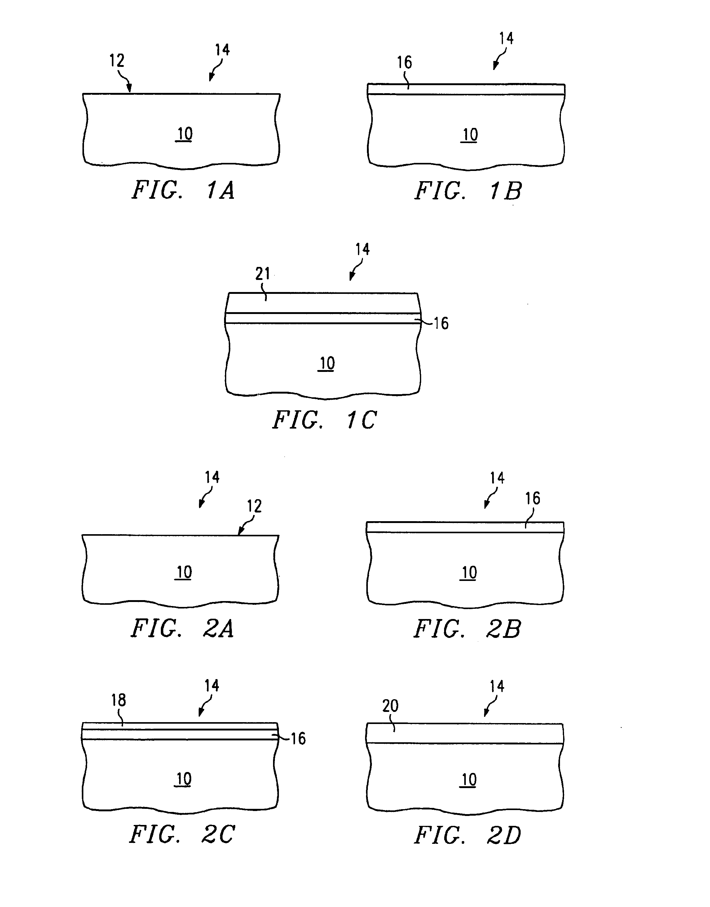
[0018]FIG. 1 outlines a method of using this invention to form a very thin, uniform SiO2 gate dielectric on a silicon substrate. Initially, Si substrate 10 with a clean surface 12 is provided. Typically, this substrate 10 will include a partially completed integrated circuit with part of the surface 12 being either bare or hydrogen passivated silicon. This surface 12 may already have structures, such as field oxide regions, already formed upon it, and other structures, such as diffusion regions formed in the substrate beneath it.

[0019]We have found that a smooth, flat silicon surface tends to grow a more uniform oxide (particularly for very thin oxides) with this method. Thus, although a hydrogen terminated silicon surface usually produces acceptable results, many very thin, highly uniform silicon dioxide gate dielectrics prefer a silicon underlayer that approaches an atomically flat or atomically stepped surface. For our purposes, an atomically stepped surface will have a very low ...


PUM

PropertyMeasurementUnit
thicknessaaaaaaaaaa
thicknessaaaaaaaaaa
thicknessaaaaaaaaaa

Abstract

This invention pertains generally to forming thin oxides at low temperatures, and more particularly to forming uniformly thick, thin oxides. We disclose a low temperature method for forming a thin, uniform oxide 16 on a silicon surface 12. This method includes providing a partially completed integrated circuit on a semiconductor substrate 10 with a clean, hydrogen terminated or atomically flat, silicon surface 12; and stabilizing the substrate at a first temperature. The method further includes exposing the silicon surface to an atmosphere 14 including ozone, while maintaining the substrate 10 at the first temperature. In this method, the exposing step creates a uniformly thick, oxide film 16. This method is suitable for room temperature processing.

Description

CROSS-REFERENCE TO RELATED APPLICATIONS[0001]This application is a continuation-in-part of application Ser. No. 08 / 904,009, titled Method For Thin Film Deposition On Single-Crystal Semiconductor Substrates, filed Jul. 31, 1997 now U.S. Pat. No. 6,020,247. This application claims the benefit of priority from U.S. provisional application 60 / 063,010, titled Low Temperature Method for Forming a Thin, Uniform Oxide, filed Oct. 23, 1997.FIELD OF THE INVENTION[0002]This invention pertains generally to forming thin oxides at low temperatures, and more particularly to forming thin, uniform oxides.BACKGROUND OF THE INVENTION[0003]Semiconductors are widely used in integrated circuits for electronic devices such as computers and televisions. These integrated circuits typically combine many transistors on a single crystal silicon chip to perform complex functions and store data. Semiconductor and electronics manufacturers, as well as end users, desire integrated circuits that can accomplish more...

Claims


Application Information

Patent Timeline
Patent Type & Authority Patents(United States)
IPC IPC(8): H01L21/31H01L21/469
CPCH01L21/02238H01L21/02255H01L29/7833H01L21/31662H01L29/51H01L21/28211
Inventor WILK, GLEN D.WALLACE, ROBERT M.BRAR, BERINDER P. S.
Owner TEXAS INSTR INC
Learn More