Semiconductor package having built-in micro electric mechanical system and manufacturing method thereof
Inactive Publication Date: 2006-04-18
AOI ELECTRONICS CO LTD
View PDF11 Cites 48 Cited by
Summary
Abstract
Description
Claims
Application Information
AI Technical Summary
This helps you quickly interpret patents by identifying the three key elements:
Problems solved by technology
Method used
Benefits of technology
Problems solved by technology
Since such an MEMS component is not a component integral with a semiconductor package, use of the MEMS component enlarges the mounting area and cannot miniaturize the semiconductor package as a whole.
Method used
Image
Click on the blue label to locate the original text in one second.
Reading with bidirectional positioning of images and text.
Examples
first embodiment
[0034](First Embodiment)
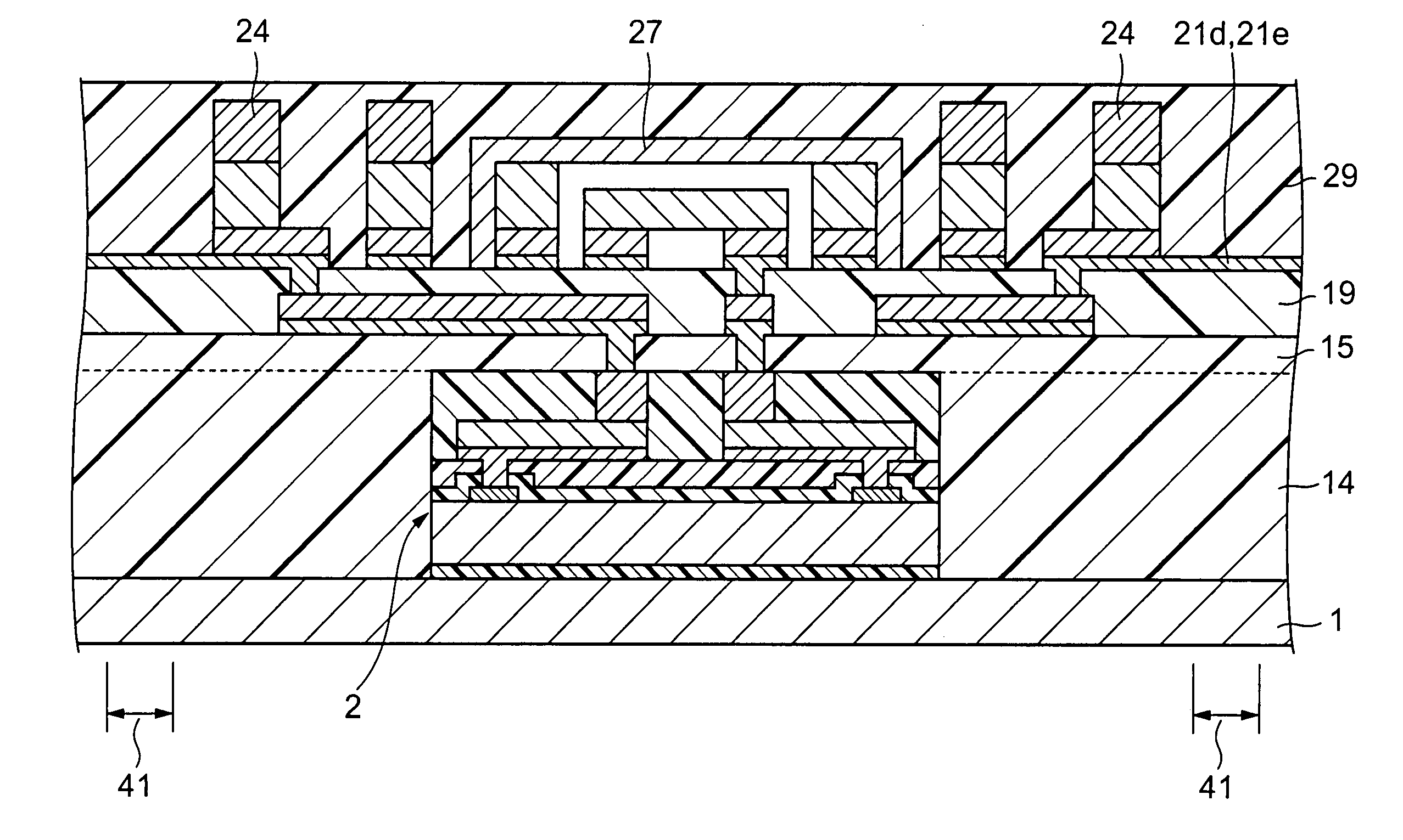
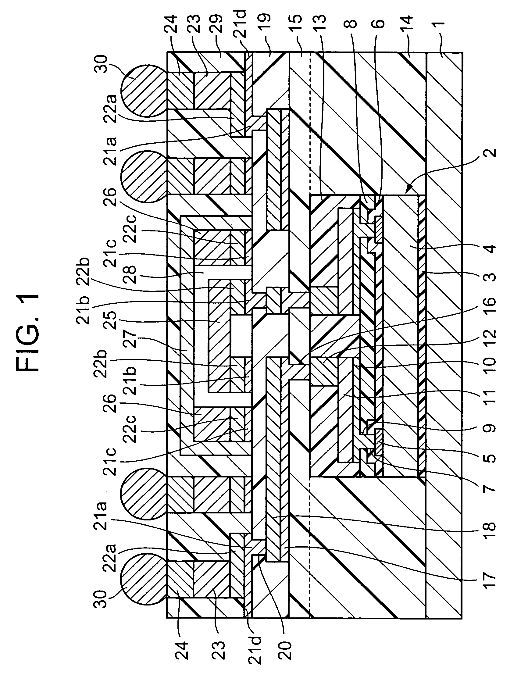
[0035]FIG. 1 is a cross-sectional view of a semiconductor package as a first embodiment of the present invention. This semiconductor package comprises a planar rectangular base plate 1 made of silicon, glass, ceramics, resin, metal, or the like. The lower surface of a planar rectangular semiconductor structure 2 having a size smaller to some degree than that of the base plate 1 is adhered to the central region of the upper surface of the base plate 1 by an adhesive layer 3 made of a die-bonding material.
[0036]The semiconductor structure 2 comprises wirings, pole electrodes, and sealing films which are described later, and is generally called a CSP (Chip Size Package). In particular, the semiconductor structure 2 is also called a wafer level CSP (W-CSP) because, as will be described later, the semiconductor structure 2 is manufactured in a manner that wirings, pole electrodes, and sealing films are formed on a siliconwafer, and each unit semiconductor structu...
second embodiment
[0073](Second Embodiment)
[0074]In the above-described first embodiment, a rectangular cylindrical cover that is capped at one end is used as the protection cover 27, and this protection cover 27 is arranged by being positioned based on the dummy pole electrodes 26, as has been explained above. However, the manner of arranging the protection cover 27 is not limited to this. For example, as the second embodiment of the present invention shown in FIG. 23, a frame-like side wall 61 may be formed by electrolytic plating of copper upon the dummy base metallayers 21c and dummy wirings 22c which are formed like a rectangular frame around the region where the planar rectangular MEMS components 25 is formed, and a flat plate 62 made of resin, metal, or the like may be adhered onto the frame-like side wall 61.
third embodiment
[0075](Third Embodiment)
[0076]In the above-described first embodiment, a case where the upper wiring includes two layers has been explained. However, the present invention is not limited to this, but the upper wiring may include three or more layers. Further, as the third embodiment of the present invention shown in FIG. 24, the upper wiring may include a single layer. The major difference between the third embodiment and the first embodiment shown in FIG. 1 is that in the third embodiment, the first upper base metal layer 17, the first upper wiring 18, and the second upper insulation film 19 shown in FIG. 1 are omitted. In this case, in order to secure routing areas for the upper wirings 21a and 21b upon the first upper insulation film 15 on the semiconductor structure 2, the MEMS component 25 is positioned biasedly to one side of the first upper insulation film 15.
[0077](Other Embodiments)
[0078]In the above-described embodiments, the MEMS component 25 and the protection cover 27 a...
PUM
Abstract
A semiconductorpackage includes a semiconductor structure having a plurality of electrodes for external connection which are provided on a semiconductor substrate, an insulation layer provided on the semiconductor structure, an upper wiring having connection pad portions and provided on the insulation layer such that at least parts of the upper wiring are connected to the electrodes for external connection of the semiconductor structure, a micro electric mechanical system electrically connected to parts of the connection pad portions of the upper wiring, pole electrodes provided so as to be electrically connected to other connection pad portions of the upper wiring, and an upper insulation film covering the vicinities of the pole electrodes and at least the vicinity of the micro electric mechanical system.
Description
BACKGROUND OF THE INVENTION[0001]1. Field of the Invention[0002]The present invention relates to a semiconductor package having a built-in Micro Electric Mechanical System, and to a manufacturing method thereof.[0003]2. Description of the Related Art[0004]Conventionally, as disclosed in Unexamined Japanese Patent Application KOKAI Publication No. 2002-57291, there is such a semiconductor package in which on a semiconductor substrate, a first conductive layer, a dielectric layer, and a second conductive layer are stacked to form a three-dimensional capacitor element, a pole electrode is formed on the capacitor element, and the pole electrode including the capacitor element is covered with a sealing film. Since this semiconductor package has the three-dimensional capacitor element formed on the semiconductor substrate, the package can be miniaturized as a whole, as compared with a case where the three-dimensional capacitor element is mounted on a circuit board.[0005]Recently, MEMS (Mi...
Claims
Application Information
Patent Timeline
Application Date:The date an application was filed.
Publication Date:The date a patent or application was officially published.
First Publication Date:The earliest publication date of a patent with the same application number.
Issue Date:Publication date of the patent grant document.
PCT Entry Date:The Entry date of PCT National Phase.
Estimated Expiry Date:The statutory expiry date of a patent right according to the Patent Law, and it is the longest term of protection that the patent right can achieve without the termination of the patent right due to other reasons(Term extension factor has been taken into account ).
Invalid Date:Actual expiry date is based on effective date or publication date of legal transaction data of invalid patent.

