Method for manufacturing wafer level chip scale package using redistribution substrate

a technology of scale package and scale substrate, which is applied in the direction of semiconductor devices, semiconductor/solid-state device details, electrical apparatus, etc., can solve the problems of reducing the chip count in a single wafer, restricting pattern design flexibility, and many new challenges to the structural and electrical design of the package rather than the chip, etc., to achieve excellent pattern design flexibility, without increasing the width of the scribe region

Inactive Publication Date: 2006-04-13
EPWORKS
View PDF3 Cites 134 Cited by
  • Summary
  • Abstract
  • Description
  • Claims
  • Application Information

AI Technical Summary

Benefits of technology

[0022] Exemplary, non-limiting embodiments of the present invention provide a method for manufacturing a wafer level chip scale package without increasing the width of a scribe region in a wafer. Exemplary, non-limiting embodiments of the present invention further provide a method for manufacturing a wafer level chip scale package not only being favorable for a reduction in package size, but also having excellent pattern design flexibility.

Problems solved by technology

Such currents of the market are reflected in reduced chip size, increased electrical terminals, and so forth, which result in many new challenges to structural and electrical design of the package rather than of the chip.
Unfortunately, this may cause a decrease in chip count in a single wafer.
Moreover, the patterned lead layer directly running on the chip edges only may restrict the pattern design flexibility.

Method used


Image

  • Method for manufacturing wafer level chip scale package using redistribution substrate
  • Method for manufacturing wafer level chip scale package using redistribution substrate
  • Method for manufacturing wafer level chip scale package using redistribution substrate

Examples


Embodiment Construction

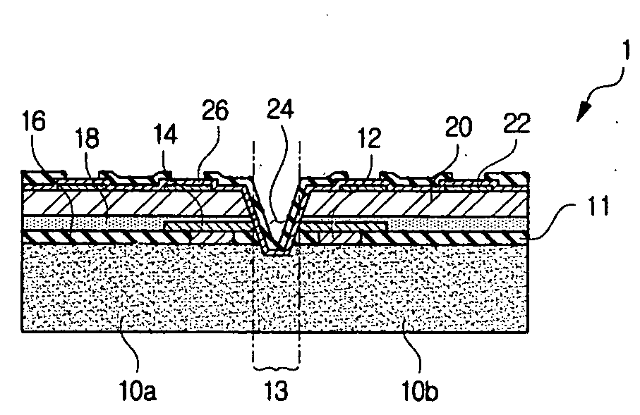
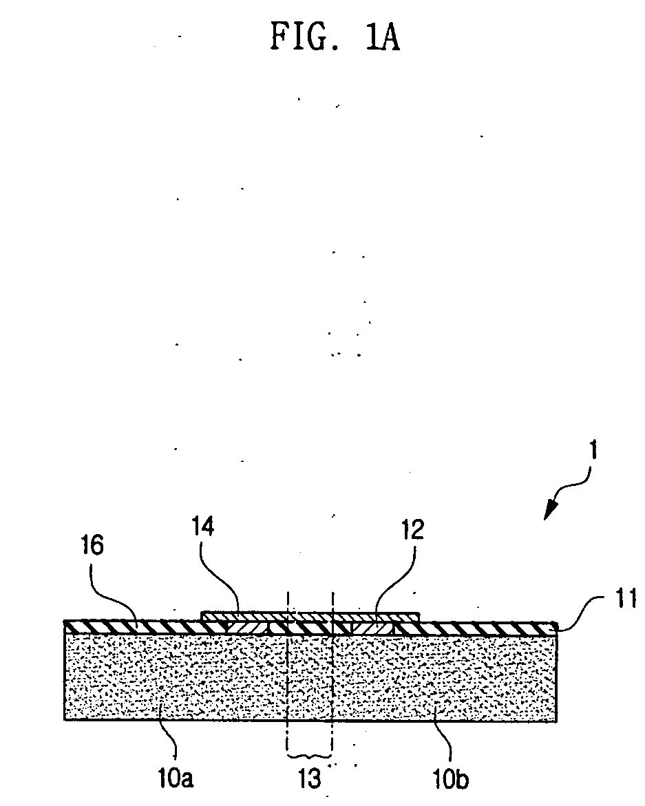
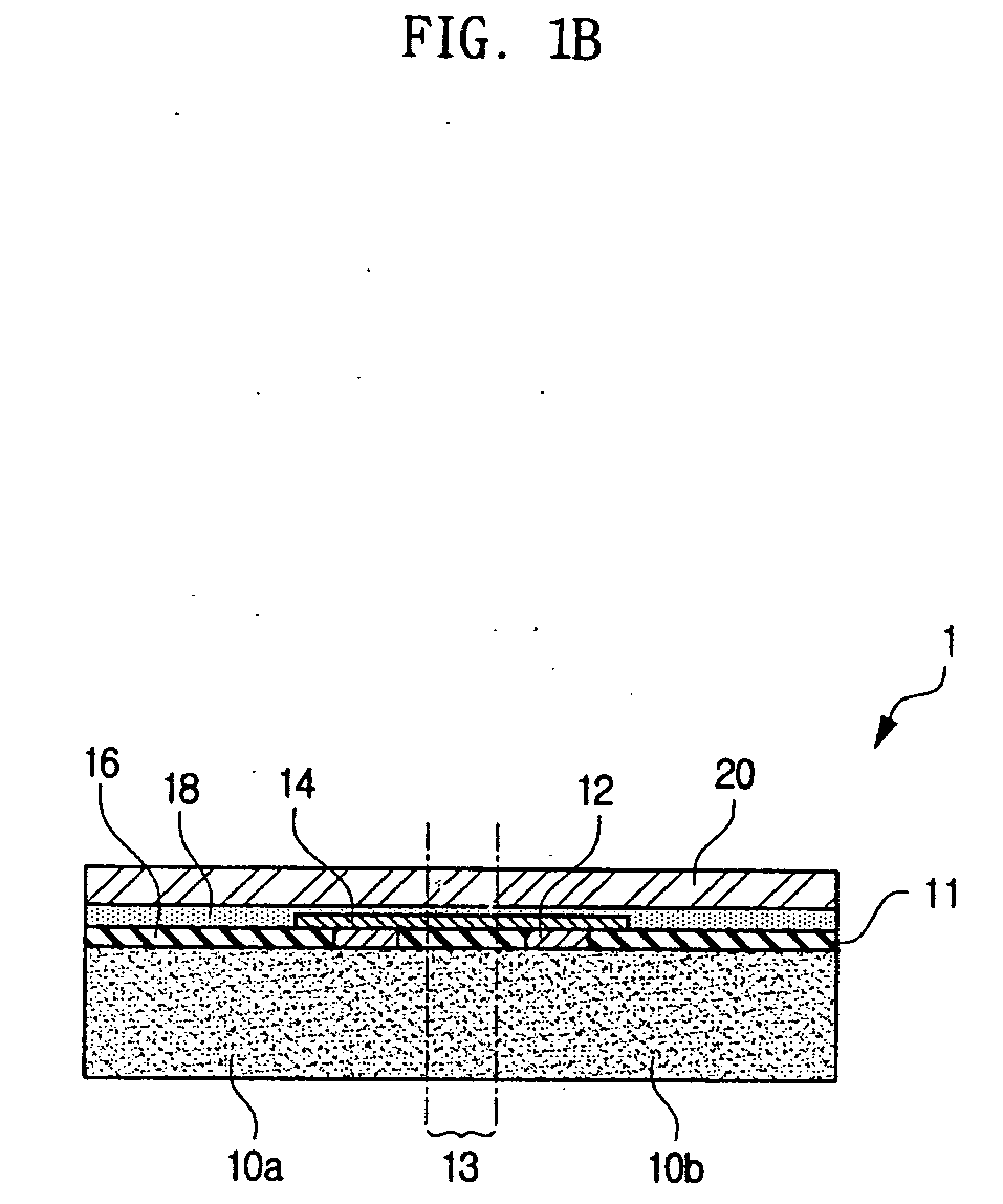
[0040] Exemplary, non-limiting embodiments of the present invention will now be described more fully hereinafter with reference to the accompanying drawings. This invention may, however, be embodied in many different forms and should not be construed as limited to the exemplary embodiments set forth herein. Rather, the disclosed embodiments are provided so that this disclosure will be thorough and complete, and will fully convey the scope of the invention to those skilled in the art. The principles and features of this invention may be employed in varied and numerous embodiments without departing from the scope of the invention.

[0041] In is noted that well-known structures and processes are not described or illustrated in detail to avoid obscuring the essence of the present invention. It is also noted that the figures are not drawn to scale. Rather, for simplicity and clarity of illustration, the dimensions of some of the elements are exaggerated relative to other elements. Like re...


PUM


Abstract

The present invention provides a method for manufacturing a wafer level chip scale package using a redistribution substrate, which has patterned bump pairs connected by redistribution lines and formed on a transparent insulating substrate. The redistribution substrate is produced separately from a wafer and then bonded to the wafer. One part of each bump pair is in contact with a chip pad on the active surface of the wafer, and the other part coincides with one of holes formed in the wafer. Conductive lines are formed in the holes and on the non-active surface of the wafer. External connection terminals are formed on the conductive lines at the non-active surface.

Description

CLAIM OF PRIORITY [0001] This application claims priority from Republic of Korea Patent Application No. 2004-0080155 filed 8 Oct. 2004 to the same inventor. BACKGROUND OF THE INVENTION [0002] 1. Field of the Invention [0003] The present invention relates generally to semiconductor packaging technology and, more particularly, to a method for manufacturing a wafer level chip scale package (WL-CSP). [0004] 2. Description of the Related Art [0005] As well known in the art, a great number of integrated circuit (IC) devices are fabricated in a semiconductor wafer and divided into individual chips. The chips are then separated from the wafer and assembled in the package form to be used for electronic systems or products. A package provides in general a structure to mechanically support the chip, a physical housing to protect the chip from the environment, electrical connections to and from the chip, and paths of removing heat generated by the chip. [0006] Recently the rapid growth of multi...

Claims


Application Information

Patent Timeline
Patent Type & Authority Applications(United States)
IPC IPC(8): H01L21/44
CPCH01L23/3114H01L23/525H01L24/13H01L24/10H01L27/14618H01L27/14632H01L27/14687H01L2224/13099H01L2924/01005H01L2924/01013H01L2924/01015H01L2924/01016H01L2924/01022H01L2924/01029H01L2924/01033H01L2924/0104H01L2924/01049H01L2924/01074H01L2924/01078H01L2924/01079H01L2924/01082H01L2924/14H01L2924/01006H01L2924/01019H01L2924/01024H01L2924/01047H01L2924/014H01L2924/00H01L2224/13H01L2224/05027H01L2224/05024H01L2224/05008H01L2224/05022H01L2224/05567H01L2224/05568H01L2224/05023H01L2224/05001H01L2224/05111H01L2224/05124H01L2224/05144H01L2224/05147H01L2224/05155H01L2224/05647H01L2224/05655H01L2224/05666H01L2224/05671H01L2224/05684H01L2224/02371H01L24/05H01L2924/00014H01L21/78H01L23/48
Inventor KIM, JAE-JUNE
Owner EPWORKS
Why Eureka
Try Eureka