Radio frequency (RF) circuit board topology

a radio frequency and circuit board technology, applied in waveguides, high frequency circuit adaptations, instruments, etc., can solve the problems of increasing complexity increasing the size of printed circuit boards, chip levels continue to decrease, and design engineers today face more and more challenges, so as to ease the congestion of routing signal traces and mitigate the effect of impedance discontinuities

Active Publication Date: 2006-04-18
TELEFON AB LM ERICSSON (PUBL)
View PDF18 Cites 114 Cited by
  • Summary
  • Abstract
  • Description
  • Claims
  • Application Information

AI Technical Summary

Benefits of technology

[0012]In order to ease routing congestion of signal traces for a circuit while meeting space constraints, a signal trace on a first conductive layer may be connected to a signal trace on a second conductive later using the interconnection structure of the present invention. Advantageously, the novel interconnection structure of the present invention allows for the transmission of high frequency signals between signal traces on different conductive layers of a circuit while maintaining signal integrity. Specifically, the present invention mitigates the impedance discontinuities at signal trace-to-via transitions inherent at high frequencies.

Problems solved by technology

Design engineers today are facing more and more challenges.
Printed circuit boards are getting more and more complex as physical size at the board, package, and chip level continues to decrease.
Reducing feature size results in lower costs and faster time to market.
As aspect ratios become worse and worse and signal frequencies continue to rise—a trend certain to continue in the future—each signal trace will inevitably exhibit transmission line effects, thereby degrading the signal integrity.
However, in high frequency applications, one problem with via structures is the lack of AC electrical isolation between the vias and the remainder of the microcircuit.
Another problem is that standard via holes do not provide a controlled impedance environment at high frequencies and, therefore, present discontinuities or changes in impedance along the signal path.
Such discontinuities may cause signal reflections (or “ringing”) of high speed digital and analog signals.
Specifically, at higher frequencies, such departure from a uniform propagation structure results in parasitic elements being formed at the junctions between the circuit traces and the via itself.
Such reactive impedance will, in turn, result in an impedance mismatch at the trace-to-via junction and energy will, accordingly, be reflected back towards the source end.
Accordingly, the potential magnitude of the negative effect of the PCB design on performance increases with frequency as the parasitic elements tend to a similar magnitude to the typical lumped components used.

Method used


Image

  • Radio frequency (RF) circuit board topology
  • Radio frequency (RF) circuit board topology
  • Radio frequency (RF) circuit board topology

Examples


Embodiment Construction

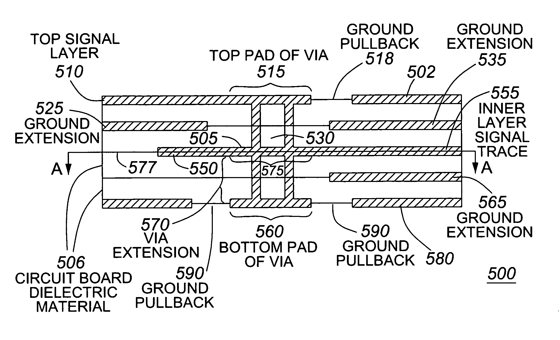
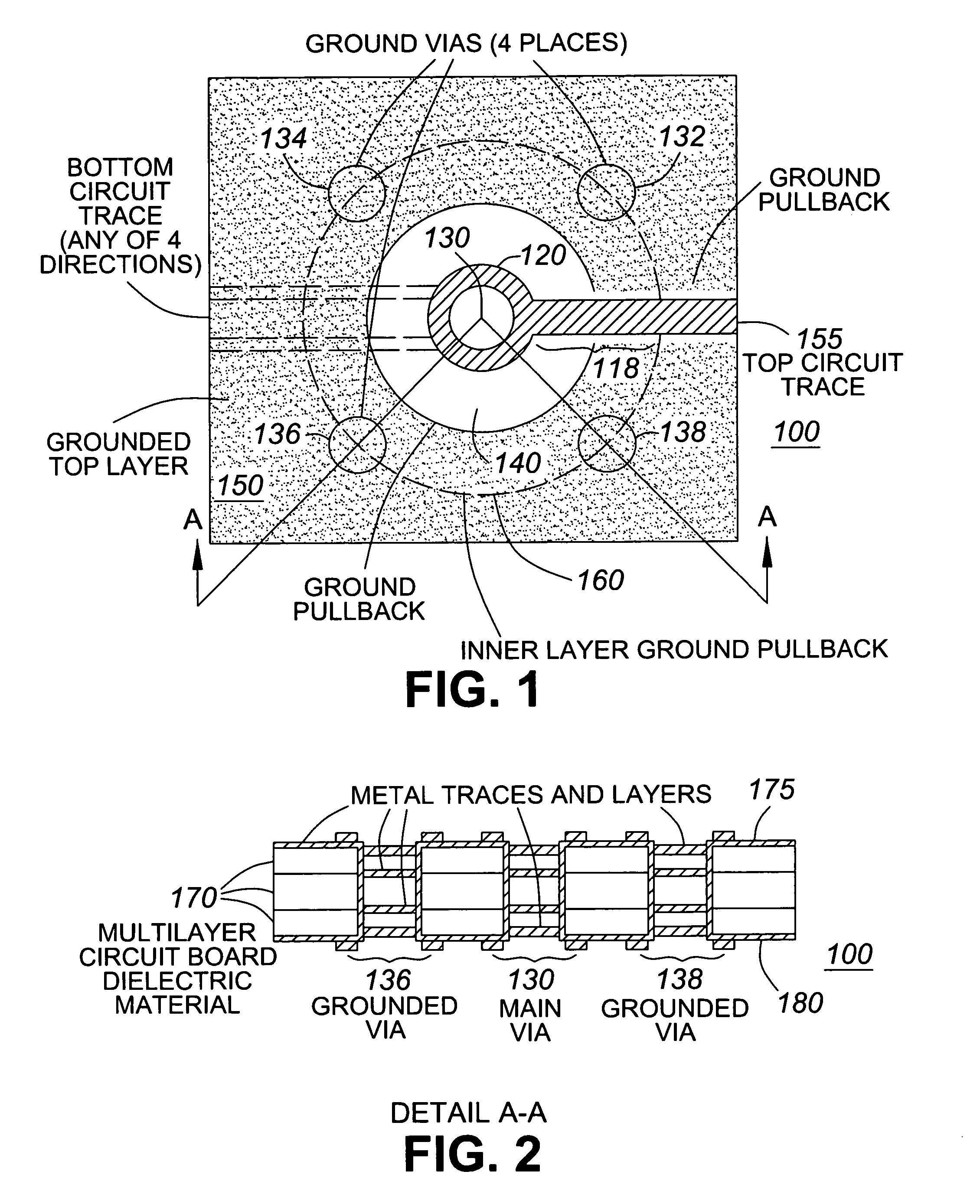
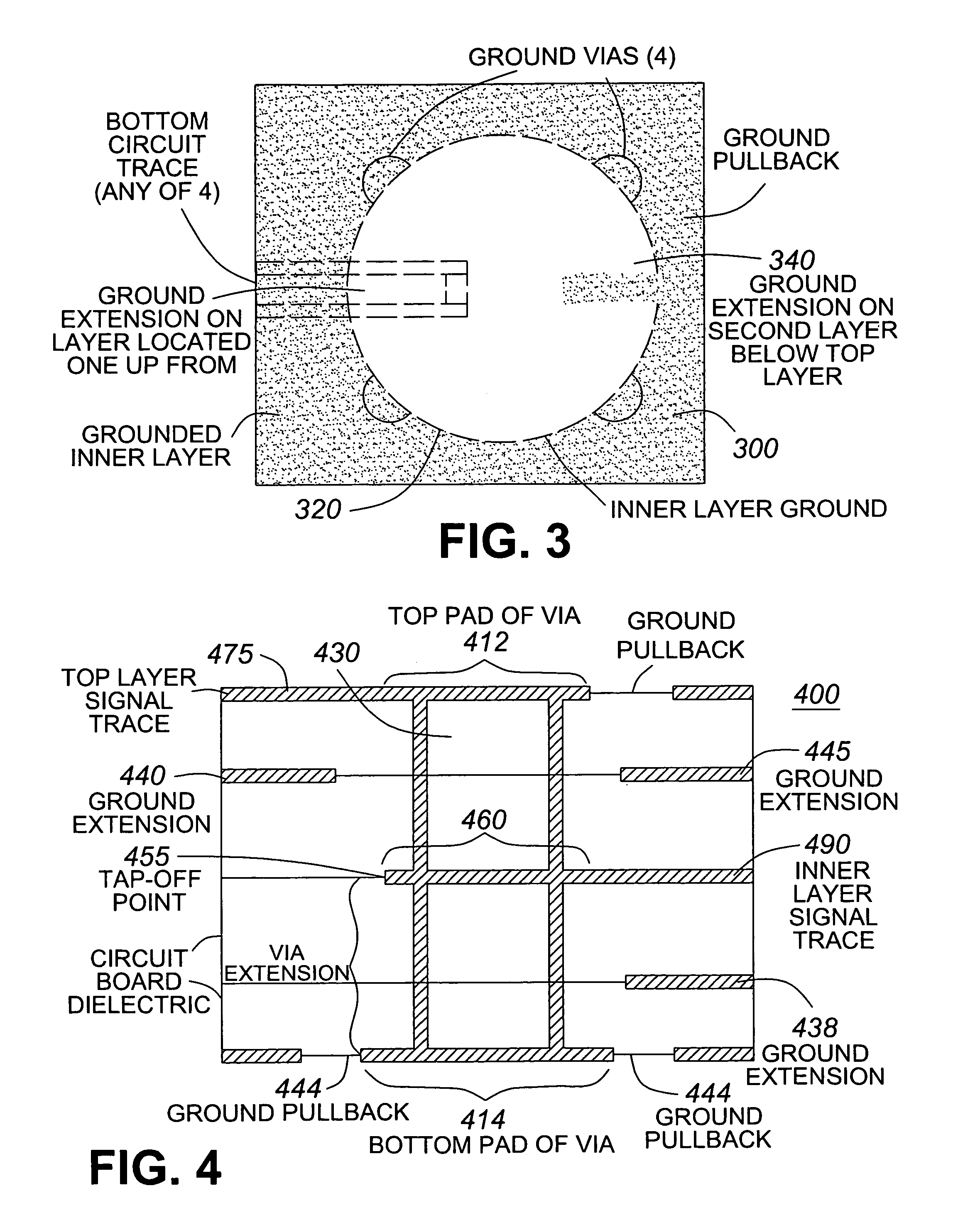
[0022]The need to move signals between various conductive layers of a printed circuit board, particularly in relation to the RF circuits used in wireless communication systems, has necessitated the creation of unique radio frequency (RF) circuit board structures to compensate for the impedance discontinuities introduced by via holes. Specifically, to generate a low reflection interface, it is necessary to compensate for the non-ideal circuit effects introduced at signal trace-to-via transition regions.

[0023]In keeping with standard transmission line theory, those skilled in the art will appreciate that, for distributed lines, the impedance per unit length is given as the square root of the ratio of the inductance per unit length divided by the capacitance per unit length (i.e. √{square root over (L / C)}). Since a standard signal conductor via has an inherent inductance per unit length, introducing a distributed capacitance per unit length will provide for a uniform impedance along th...


PUM


Abstract

An interconnection structure for interconnecting circuitry on a first conductive layer to circuitry on a second conductive layer is provided. The interconnection structure of the present invention comprises a signal conductor via surrounded by a plurality of ground vias. The plurality of ground vias shield the signal conductor via, thus providing electrical isolation for the conductor via from the rest of the circuitry. One feature of the present invention is that the plurality of ground vias can be modified, adjusting their diameters and their placement relative to the signal conductor via, in order to affect the overall characteristic impedance of the interconnection structure. This feature is useful when propagating high frequency signals between signal traces on different conductive layers of a printed circuit board. In view of the high frequencies used in today's wireless communication systems, the interconnection structure proposed aids in the practical implementation of radio frequency modules by mitigating the effects of impedance discontinuities ordinarily present at signal trace-to-via transition regions.

Description

FIELD OF THE INVENTION[0001]The present invention relates to printed circuit board design and, more particularly, to a novel circuit board topology for use in radio frequency products that mitigates the deleterious parasitic effects introduced by vias or plated through holes.BACKGROUND TO THE INVENTION[0002]Design engineers today are facing more and more challenges. Printed circuit boards are getting more and more complex as physical size at the board, package, and chip level continues to decrease. These structures are also expected to perform at higher speeds. Reducing feature size results in lower costs and faster time to market. However, high density also means more conductive metal layers and more signal traces routed on smaller and thinner boards.[0003]To facilitate electrical communication between conductive layers, a class of well known structures called vias are used. In general, vias are openings etched through dielectric layers between a first conductive layer and a second...

Claims


Application Information

Patent Timeline
Patent Type & Authority Patents(United States)
IPC IPC(8): H01P5/00G11C7/00H01L23/52H05K1/02H05K1/11H05K3/42
CPCH05K1/0222H05K1/0251H01L2223/6616H01L2223/6622H01L2223/6627H01L2924/1903H05K2201/09809H05K3/429H05K2201/0715H05K2201/09618H05K2201/09718
Inventor BRUNETTE, GILBERT P.JOHNSON, ERICRAYMENT, STEPHEN G.SOUL, COLIN
Owner TELEFON AB LM ERICSSON (PUBL)
Why Eureka
Try Eureka