
Using electro-magnetically induced transparency in photonic crystal cavities to obtain large non-linear effects

a photonic crystal and electro-magnetically induced technology, applied in the field of solid-state-based electromagnetically induced transparency (eit), can solve the problems of increasing the power level of the long-haul network, affecting and almost 90% of the cost of any long-haul network is in the module that performs electro-optical conversion, so as to increase the non-linear properties of the photonic crystal and increase the non-linear properties of the photo

Inactive Publication Date: 2006-04-18
MASSACHUSETTS INST OF TECH +1
View PDF1 Cites 12 Cited by
  • Summary
  • Abstract
  • Description
  • Claims
  • Application Information

AI Technical Summary

Benefits of technology

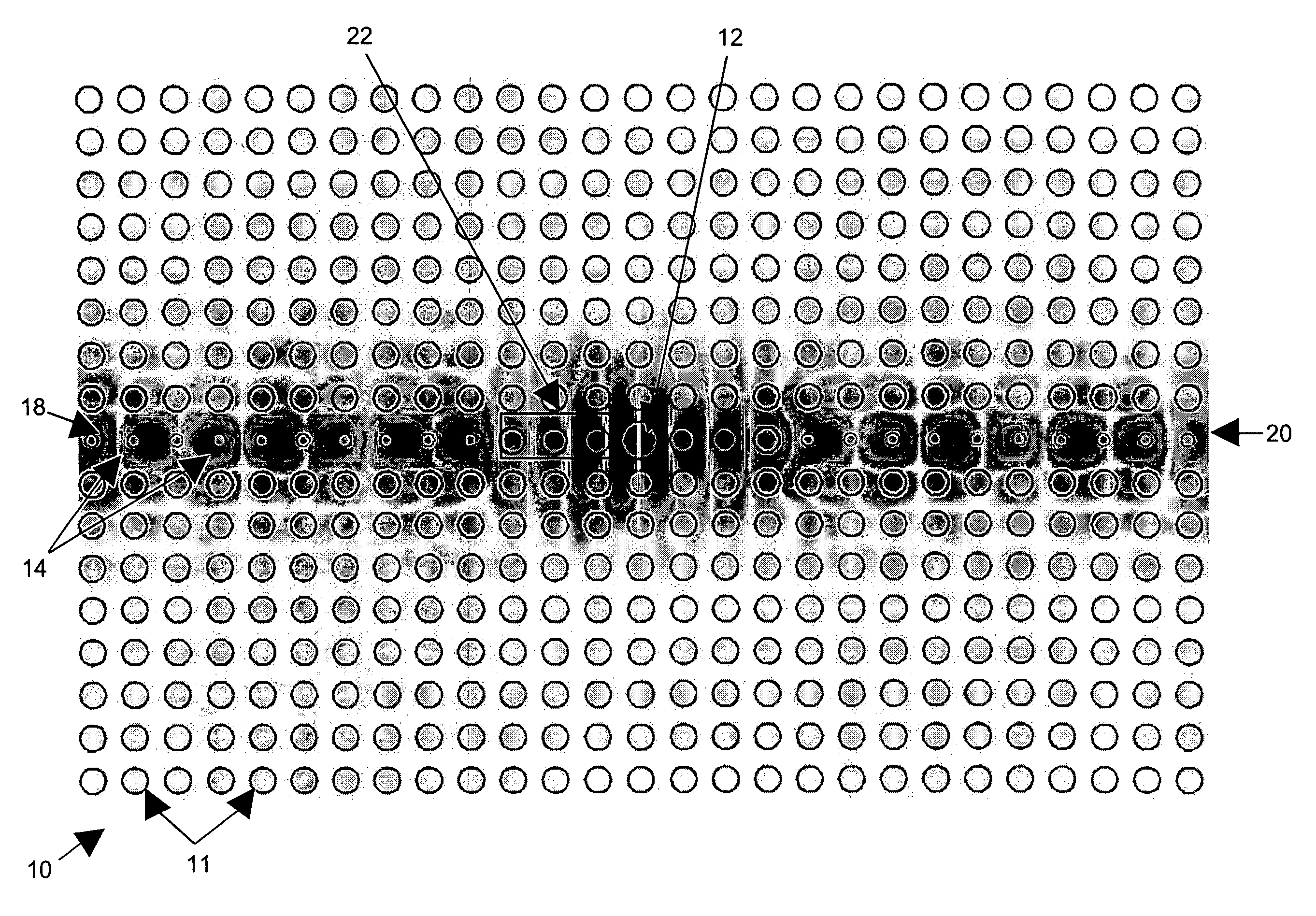
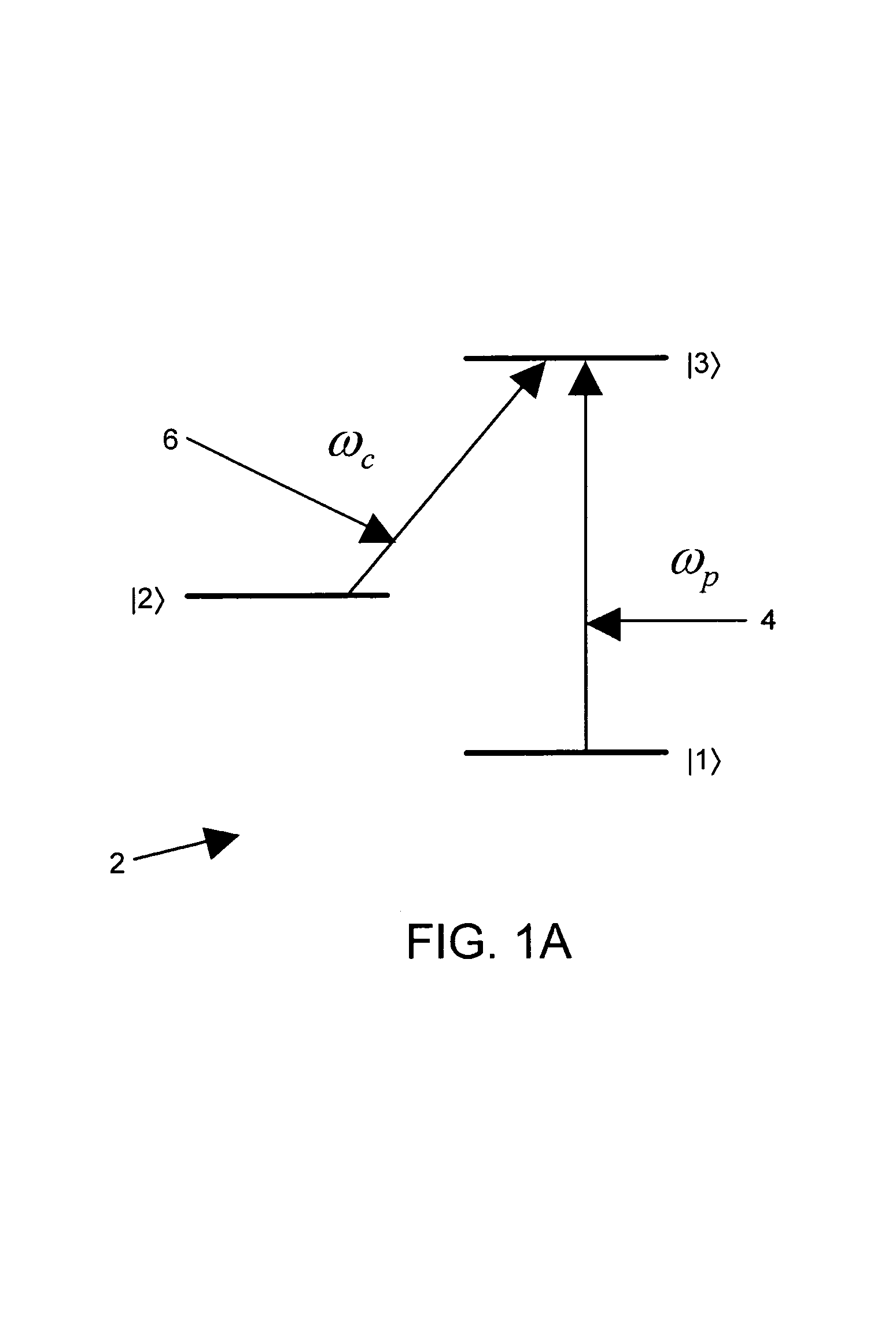
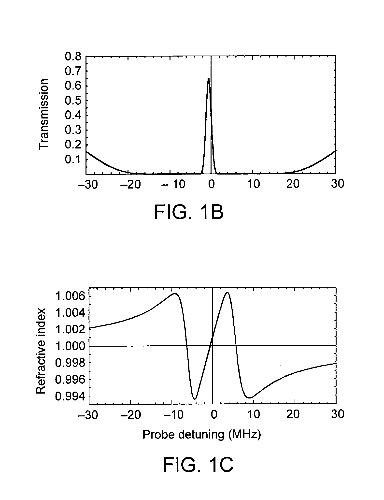
[0014]According to one aspect of the invention, there is provided a photonic crystal system. The photonic crystal system includes a microcavity inside it. The photonic crystal structure is doped with materials that exhibit electromagnetic induced transparency (EIT) so as to increase the non-linear properties of the photonic crystal.
[0015]According to another aspect of the invention, there is provided a method of forming a microcavity structure inside of a photonic crystal, which is doped with materials that exhibit electromagnetic induced transparency (EIT) so as to increase the non-linear properties of the photonic crystals.

Problems solved by technology

There are various physical reasons that prevent electronics from functioning well at so high frequencies, making such electronics extremely expensive.
In fact, almost 90% of the cost of any long-haul network lies in modules that perform electro-optical conversion.
Unfortunately, in experimental integrated all-optical devices that achieve the desired performance today, much higher power levels are needed.
Although quantum information can be transferred from one system (e.g. photons) into another (e.g. electrons), and then back, such transfers are technologically challenging.
Unfortunately, the power requirements needed to obtain large enough non-linearities to realize this scheme with the solutions that existed at the time were many orders of magnitude too large for all-optical computing to be feasible.
Clearly, this scheme is not feasible.
Unfortunately, this approach cannot be used if ultra-fast operation is desired.
Still, improvements of more than one order of magnitude are un-feasible, and such materials are typically difficult to work with and difficult to integrate with other optical materials on the same chip.
Unfortunately, this approach is necessarily accompanied with enormously large absorption of the optical beam.
Furthermore, since this is a resonant phenomenon, the response and recovery times are necessarily large.
This approach has been successfully used for many applications, but typically imposes some serious constraints.
Also, silica is a particularly bad non-linear material; materials used in integrated optics typically have Kerr coefficients almost three orders of magnitude larger than silica.

Method used


Image

  • Using electro-magnetically induced transparency in photonic crystal cavities to obtain large non-linear effects
  • Using electro-magnetically induced transparency in photonic crystal cavities to obtain large non-linear effects
  • Using electro-magnetically induced transparency in photonic crystal cavities to obtain large non-linear effects

Examples


Embodiment Construction

[0022]Photonic crystals are particularly suitable for implementation of various structural non-linearity enhancement schemes. Photonic crystals are artificially created materials in which index of refraction varies periodically between high-index and low-index values. Any light of wavelength comparable to the periodicity of the photonic crystal is not allowed to propagate inside it. In particular, photonic crystals have so-called photonic band-gaps; any light with frequency inside a bandgap is not allowed to propagate in the material, while the frequencies above and below the bandgap are allowed to propagate freely inside the crystal. This is reminiscent of electronic band-gaps for electrons propagating in semi-conductors. Photonic crystals therefore present for photons a material very similar to what semi-conductors present for electrons. Since semi-conductors led to integration of electronics, photonic crystals are considered to be the most promising candidate to enable large-scal...


PUM

PropertyMeasurementUnit
telecommunication poweraaaaaaaaaa
poweraaaaaaaaaa
induced transparencyaaaaaaaaaa

Abstract

A photonic crystal structure includes a microcavity (point defect). The photonic crystal structure (or just the microcavity) is doped with materials that exhibit electro-magnetic induced transparency (EIT) so as to increase the non-linear properties of the photonic crystal.

Description

PRIORITY INFORMATION[0001]This application claims priority from provisional application Ser. No. 60 / 430,957 filed Dec. 4, 2002, which is incorporated herein by reference in its entirety.BACKGROUND OF THE INVENTION[0002]The invention relates to the field of solid-state based electro-magnetically induced transparency (EIT), and in particular to exploring solid-state-based electro-magnetically induced transparency (EIT) as a non-linear medium in photonic crystal cavities.[0003]In the nodes of any long-haul telecommunication network, one needs to perform electro-optical conversion in order to process optical signals. The tasks that typically need to be performed include: routing, regeneration, changing wavelengths, changing bit-rates, etc. Since bit-rates in long-haul networks are typically high (10 Gbit / s today, and 40 Gbit / s in the next generation networks), one is forced to use ultra-fast (>100 GHz for 40 Gbit / s) electronics to perform such tasks. There are various physical reason...

Claims


Application Information

Patent Timeline
Patent Type & Authority Patents(United States)
IPC IPC(8): G02B6/10G02F1/35G02F1/365
CPCG02F1/35G02F1/3515G02F1/365G02F2203/15G02F2202/32
Inventor SOLJACIC, MARINJOANNOPOULOS, JOHN D.HAU, LENE VESTERGAARD
Owner MASSACHUSETTS INST OF TECH
Learn More