Method for forming isolation layer of semiconductor device

a technology of isolation layer and semiconductor, which is applied in the manufacturing of semiconductor/solid-state devices, basic electric elements, electric devices, etc., can solve the problems of leakage characteristic deterioration, leakage characteristic deterioration of liner nitride layer, etc., and achieve the effect of preventing the deterioration of leakage characteristi

Active Publication Date: 2006-04-25
SK HYNIX INC
View PDF3 Cites 12 Cited by
  • Summary
  • Abstract
  • Description
  • Claims
  • Application Information

AI Technical Summary

Benefits of technology

[0012]Accordingly, the present invention has been made to solve the above-mentioned problems occurring in the prior art, and it is an object of the present invention to provide a method for forming isolation layer of a semiconductor device, which can prevent the deterioration of a leakage characteristic due to a liner nitride layer in a peripheral circuit region.
[0013]Another object of the present invention is to provide a method for forming isolation layer of a semiconductor device, which improves the refresh characteristic and prevents the deterioration of the leakage characteristic in a peripheral circuit region, thereby improving the reliability and properties of a device.

Problems solved by technology

Therefore, a leakage characteristic deteriorates.
However, the liner nitride layer deteriorates the leakage characteristic in the P+ well region of the peripheral circuit region.

Method used


Image

  • Method for forming isolation layer of semiconductor device
  • Method for forming isolation layer of semiconductor device
  • Method for forming isolation layer of semiconductor device

Examples


Embodiment Construction

[0022]Hereinafter, a preferred embodiment of the present invention will be described with reference to the accompanying drawings.

[0023]Hereinafter, a technical principle of the present invention will be described.

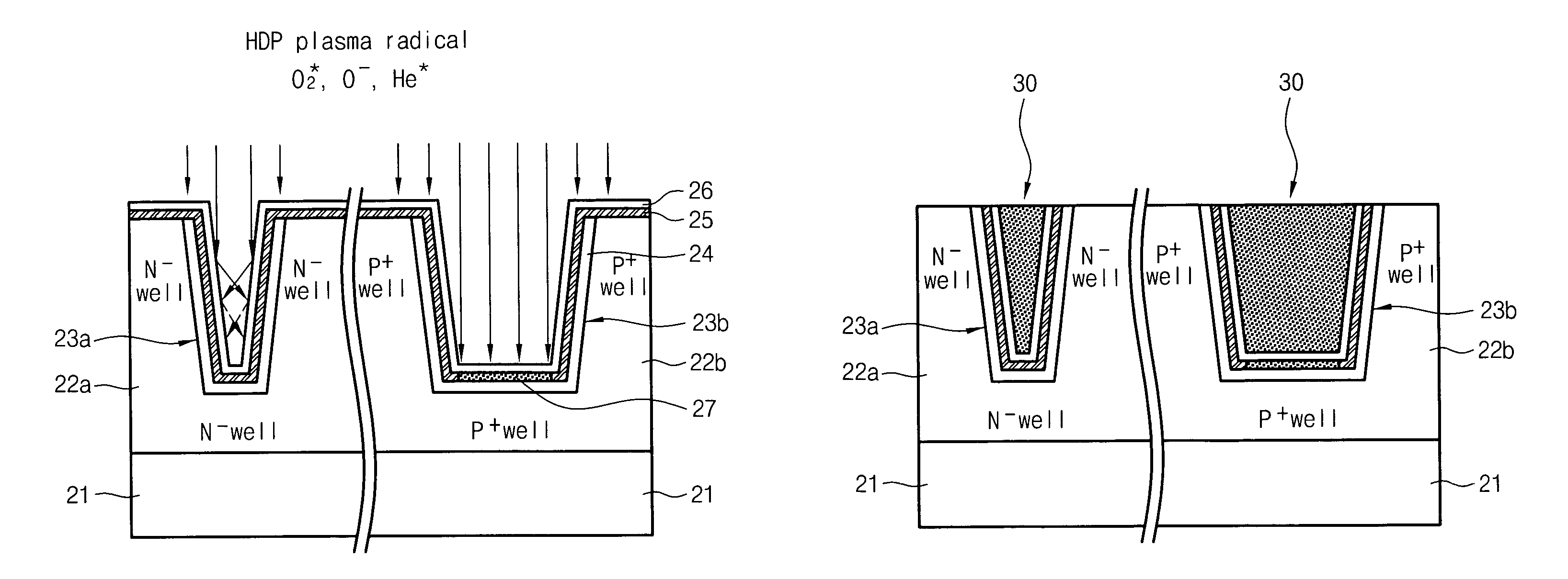
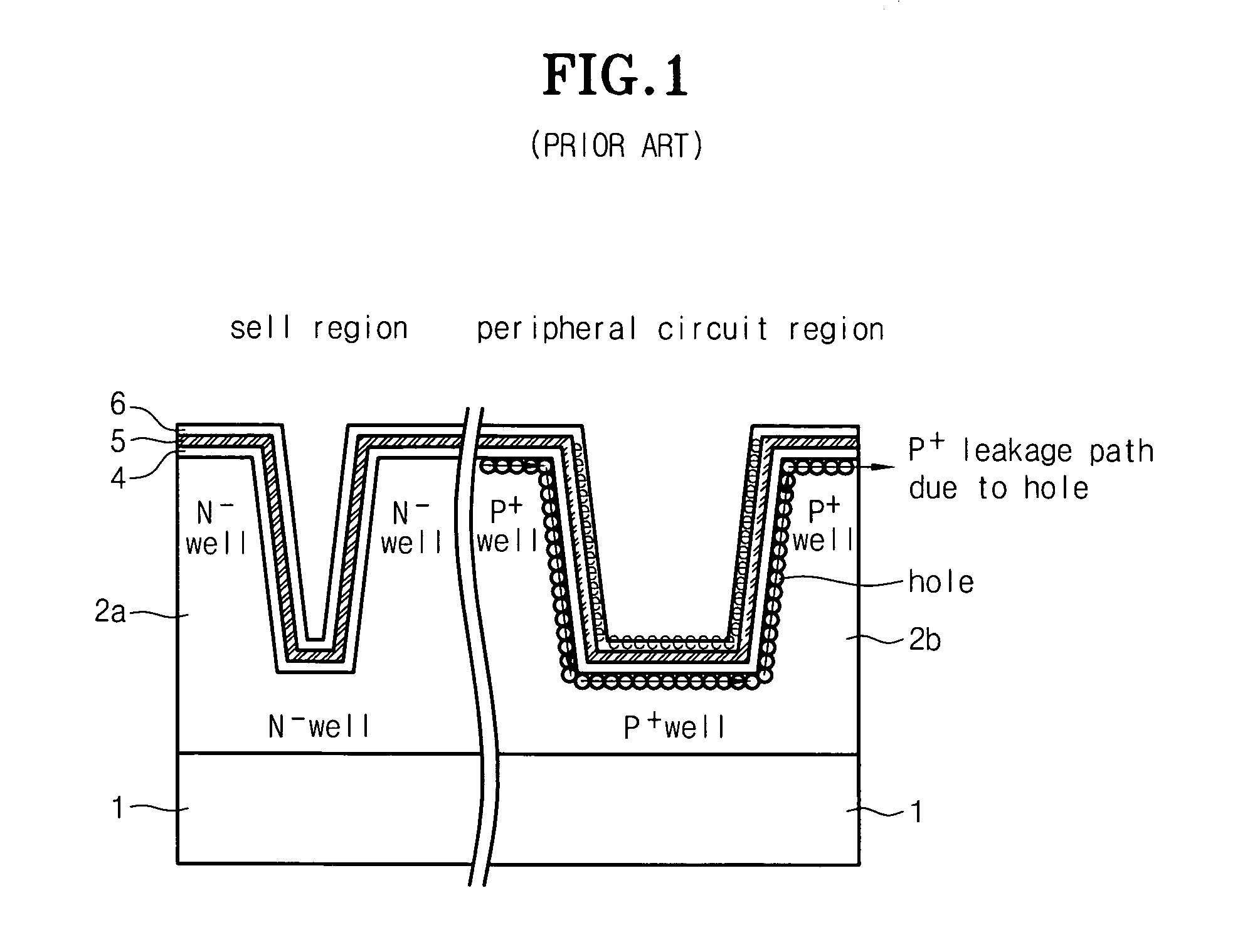
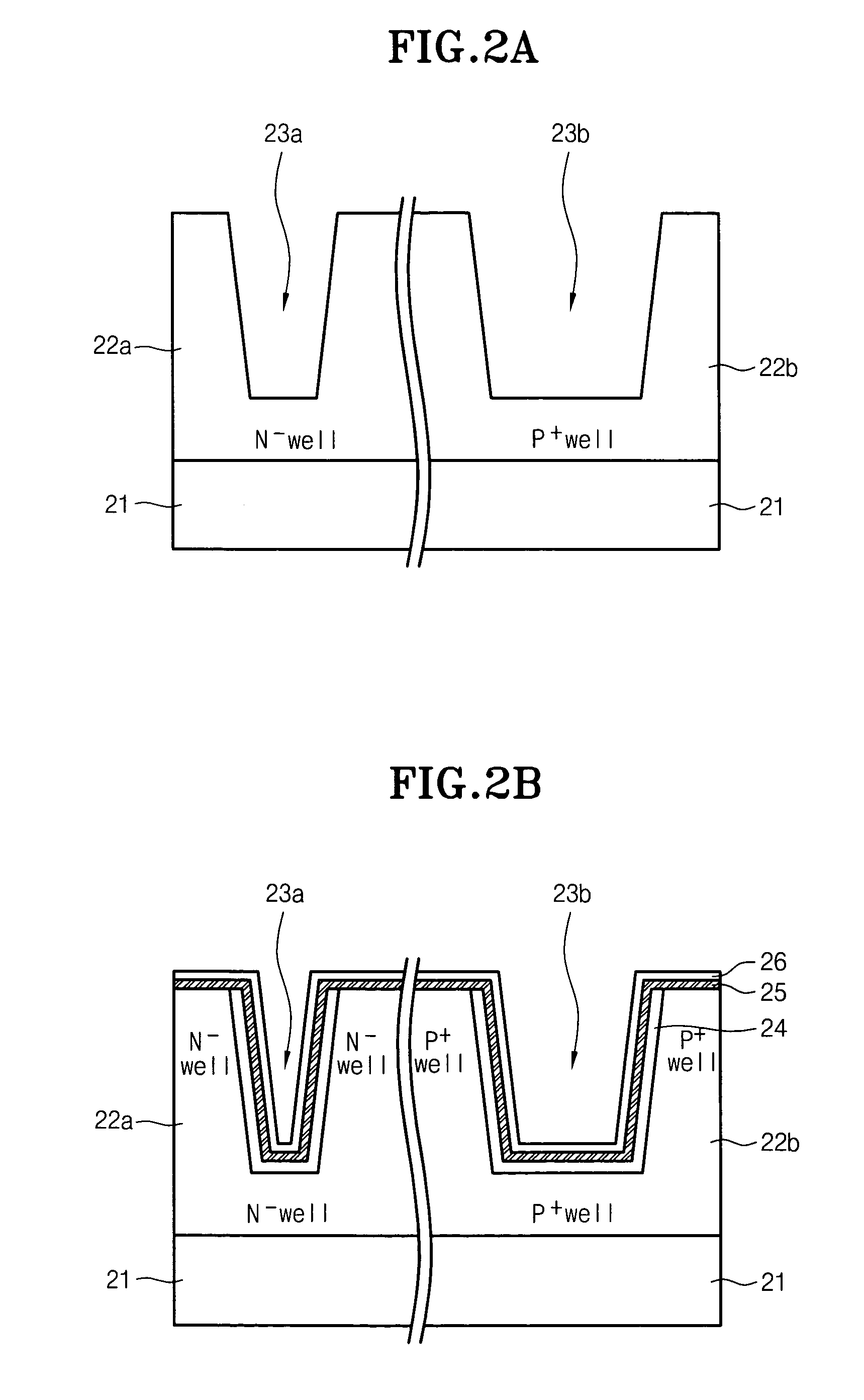
[0024]A liner nitride layer is formed to improve refresh characteristic, and it is preferred to form the liner nitride layer in a cell region. However, since the liner nitride layer deteriorates a leakage characteristic in a peripheral circuit region, it is not preferred to form the liner nitride layer in the peripheral circuit region. Accordingly, in the present invention, the liner nitride layer is formed in the cell region and the peripheral circuit region and only a portion of the liner nitride layer formed on the bottom portion of a trench in the peripheral circuit region is selectively eliminated. In this way, a P+ leakage path is eliminated, so that the deterioration of the leakage characteristic in the peripheral circuit region does not occur.

[0025]By this reason, i...


PUM


Abstract

A method for forming an isolation layer of a semiconductor device is disclosed, which comprises the steps of: etching a silicon substrate having a cell region and a peripheral circuit region, forming a first trench having a first size in the cell region, and forming a second trench having a second size, which is larger than the first size of the first trench, in the peripheral circuit region; forming a sidewall oxide layer on surfaces of the first trench and the second trench; sequentially depositing a liner nitride layer and a liner oxide layer on a resultant substrate inclusive of the sidewall oxide layer; performing a plasma pre-heating process using O2+He with respect to the resultant substrate in an HDP CVD process chamber and selectively oxidizing a portion of the liner nitride layer remaining on a bottom of the second trench in the peripheral circuit region; continuously depositing an HDP oxide layer on the resultant substrate having been subjected to the plasma pre-heating process, thereby filling the trenches; and performing a chemical mechanical polishing process with respect to the HDP oxide layer.

Description

BACKGROUND OF THE INVENTION[0001]1. Field of the Invention[0002]The present invention relates to a method for forming an isolation layer of a semiconductor device, and more particularly to a method for preventing the deterioration of a leakage characteristic due to the formation of a liner nitride layer in a peripheral circuit region.[0003]2. Description of the Prior Art[0004]In order to increase data retention time, which is retention time of data stored in a DRAM cell, that is, **to improve refresh characteristic, technology has been introduced, which forms a liner nitride layer before the deposition of an oxide layer buried in a trench in a shallow trench isolation (hereinafter, referred to as an STI) process.[0005]Herein, the improvement in the refresh characteristic is resulted from stress alleviation and diffusion prevention on an isolation layer by the liner nitride layer.[0006]Further, the formation of the liner nitride layer may be preferred in a cell region, but it causes ...

Claims


Application Information

Patent Timeline
Patent Type & Authority Patents(United States)
IPC IPC(8): H01L21/302H01L21/762
CPCH01L21/76229H01L21/762
Inventor KIM, JUNG GEUN
Owner SK HYNIX INC
Why Eureka
Try Eureka