Unlock instant, AI-driven research and patent intelligence for your innovation.

Semiconductor integrated circuit for high frequency power amplifier, electronic component for high frequency power amplifier, and radio communication system

Inactive Publication Date: 2006-04-25
RENESAS TECH CORP
View PDF4 Cites 10 Cited by
  • Summary
  • Abstract
  • Description
  • Claims
  • Application Information

AI Technical Summary

Benefits of technology

[0011]Consequently, the inventors et al. developed a technology to cope with this. The technology is implemented by providing the above current detection circuit 20 with a characteristic wherein its output is nth root-functionally changed relative to its input. More specifically, as illustrated in FIG. 13, a square root conversion circuit 30 is placed between the current detection circuit 20 and the current-voltage conversion circuit 40. Thus, change in output power Pout relative to output level instruction signal Vramp is made substantially linear, as illustrated by solid line B2 in FIG. 5(B). As a result, the control sensitivity in the region where the request-to-send level is low is enhanced.
[0015]An object of the present invention is to provide a high frequency power amplification circuit which, in a radio communication system wherein detection of output level required for the feedback control of the output power of the high frequency power amplification circuit is carried out by current detection, allows the enhancement of the stability of control loop and the response to change in the level of request-to-send, and to provide an electronic component and a radio communication system which incorporate the high frequency power amplification circuit.
[0016]Another object of the present invention is to provide a high frequency power amplification circuit which, in a radio communication system wherein detection of output level required for the feedback control of the output power of the high frequency power amplification circuit is carried out by current detection, is capable of lowering the control sensitivity in a region where the level of request-to-send is low, so that the output level can be controlled with accuracy over the entire control range, and allows the enhancement of the stability of control loop and the response to change in the level of request-to-send, and to provide an electronic component and a radio communication system which incorporate the high frequency power amplification circuit.
[0020]The above-mentioned means increases the phase margin of the open loop. The loop goes from the control-side input terminal (noninverting input terminal) of the error amplifier to which the output level instruction signal is inputted to the high frequency power amplification circuit to the current detection circuit to the current-voltage conversion circuit and back to the feedback-side input terminal (inverting input terminal) of the error amplifier. Since the phase margin of the open loop is increased, the response to change in output level instruction signal can be enhanced. At the same time, the stability of the open loop can be enhanced.
[0021]Further preferably, a square root conversion circuit is placed between the current detection circuit and the current-voltage conversion circuit. Provision of the square root conversion circuit lowers the control sensitivity of the high frequency power amplification circuit for output level instruction signals in the region where the level of request-to-send is low. As a result, the output level can be controlled with accuracy over the entire control range. Further, provision of the square root conversion circuit increases an amount of phase turn of the open loop. If this is left intact, the response to change in the level of request-to-send is degraded. However, provision of the phase compensation circuit increases the phase margin of the open loop, and thus the response of the loop to change in output level instruction signal can be enhanced.

Problems solved by technology

This makes reduction in module size difficult.
This increases a burden on set makers and is a problem.
Use of a coupler also poses another problem: a relatively large power loss is produced.

Method used


Image

  • Semiconductor integrated circuit for high frequency power amplifier, electronic component for high frequency power amplifier, and radio communication system
  • Semiconductor integrated circuit for high frequency power amplifier, electronic component for high frequency power amplifier, and radio communication system
  • Semiconductor integrated circuit for high frequency power amplifier, electronic component for high frequency power amplifier, and radio communication system

Examples


first embodiment

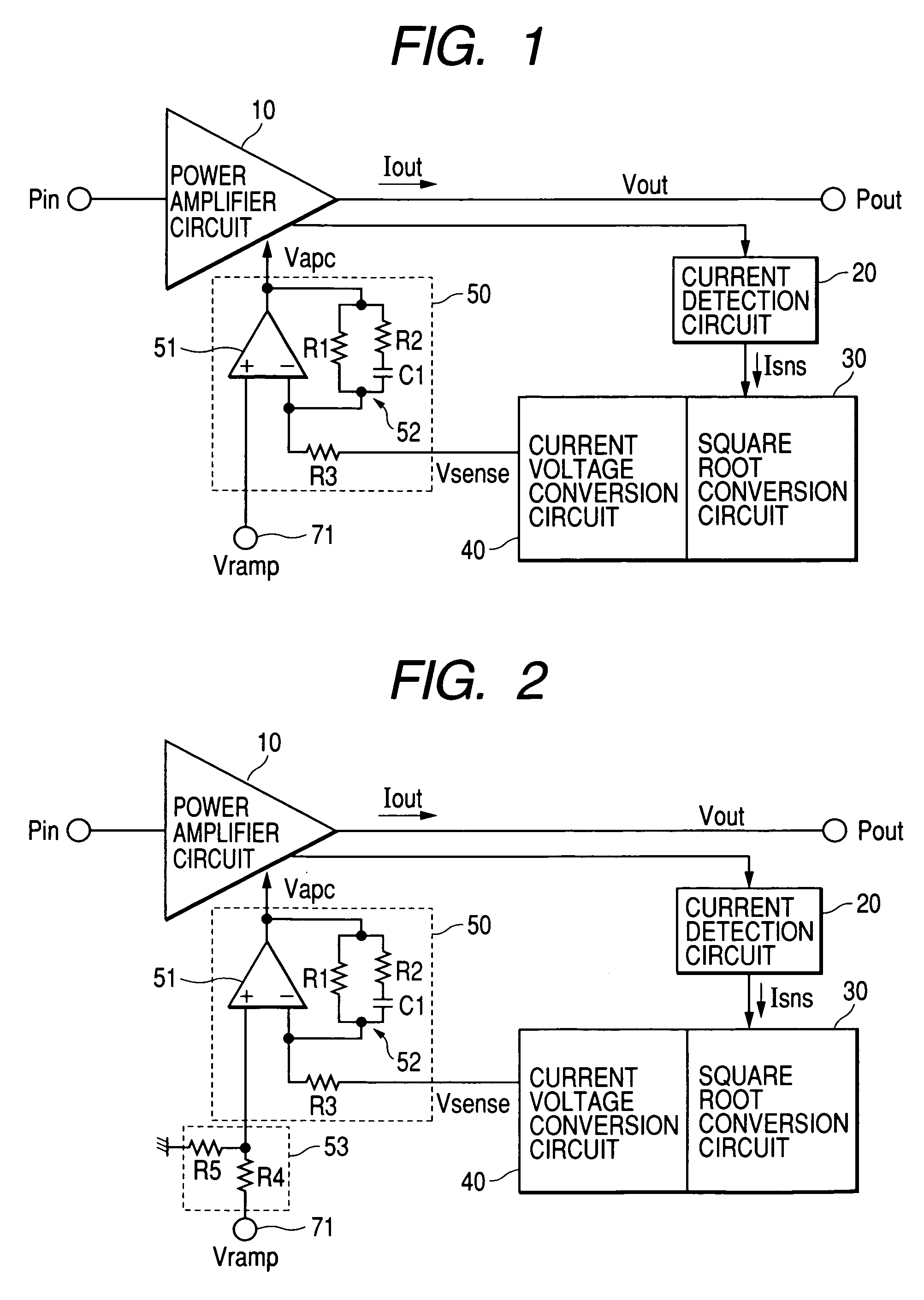
[0040]FIG. 1 schematically illustrates the constitution of the feedback control system of the high frequency power amplification circuit of current detection type to which the present invention is applied.

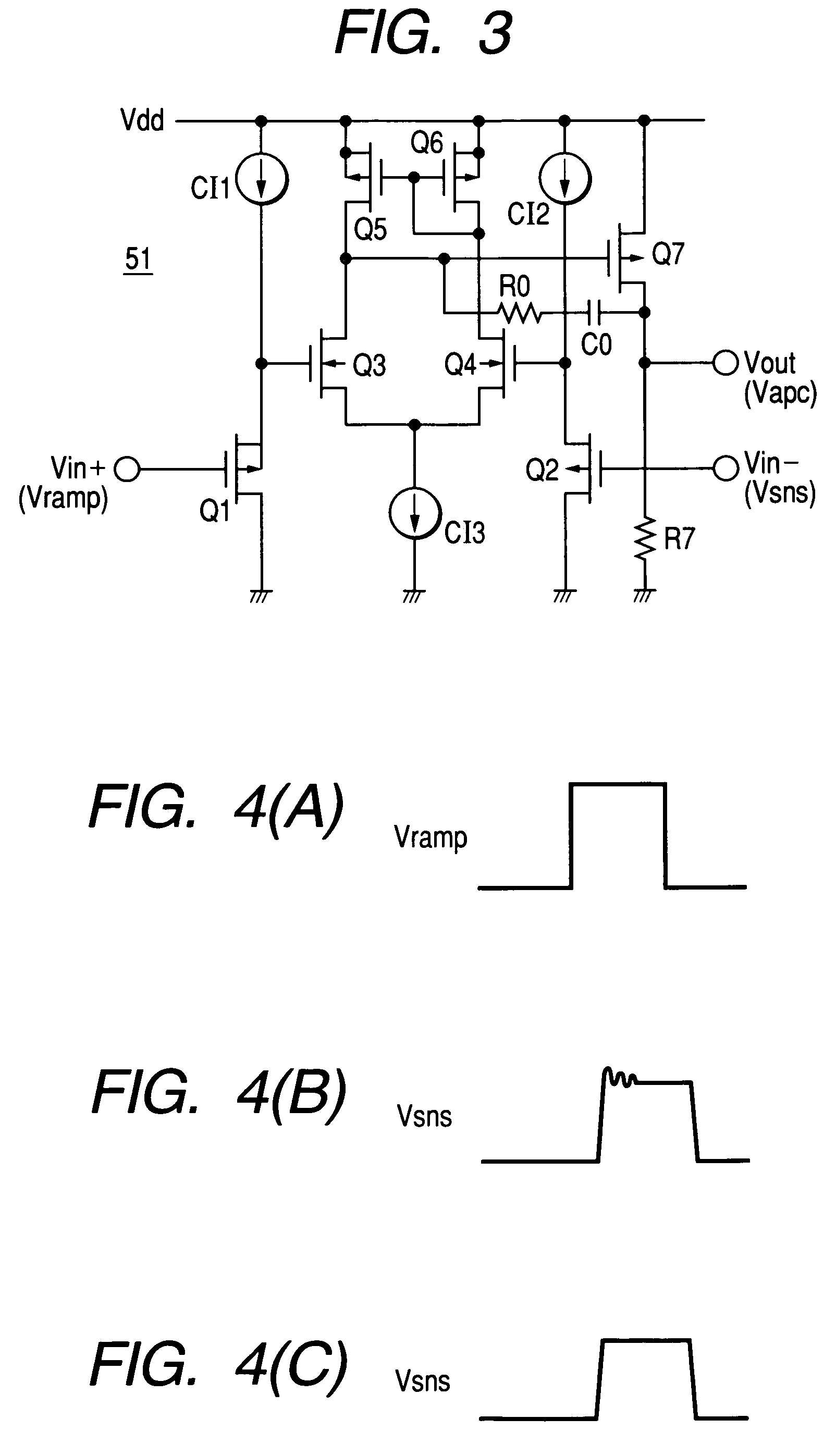
[0041]In FIG. 1, numeral 10 denotes a power amplification circuit (power amplifier) which amplifies high frequency signal Pin; numeral 20 denotes a current detection circuit which detects the output level of the power amplification circuit 10 and outputs a current corresponding to it; numeral 30 denotes a square root conversion circuit which converts a current Isns outputted from the current detection circuit 20 into a current Isout which is the second root (square root) of it; numeral 40 denotes a current-voltage conversion circuit which converts the output current Isout of the square root conversion circuit 30 into detection voltage Vsns; and numeral 50 denotes an error voltage detection circuit (error amplifier) which compares the output voltage of the current-voltage conversion...

second embodiment

[0047]FIG. 2 schematically illustrates the constitution of the feedback control system of the high frequency power amplification circuit of current detection type to which the present invention is applied. This embodiment is different from the embodiment in FIG. 1 in that an attenuator (attenuating means) 53 is provided on the noninverting input terminal side of the error amplifier 50. Provision of the attenuator 53 reduces the gain of the control system from the viewpoint of output level instruction signal Vramp.

[0048]The attenuator 53 in this embodiment comprises a resistance element R4 placed between a control terminal 71 to which output level instruction signal Vramp is inputted and the noninverting input terminal of the error amplifier 50; and a resistance element R5 placed between the node of the resistance element R4 on the opposite side to the control terminal 71 and a grounding point. Therefore, the attenuator 53 in this embodiment can be considered as resistance type volta...


PUM


Abstract

In a radio communication system, an electronic component for high frequency power amplifier carries out the detection of output level, required for feedback control of the output power of a high frequency power amplification circuit, by current detection. The electronic component has an error amplifier. The error amplifier compares an output level detection signal with an output level instruction signal, and generates a signal for controlling the gain of the high frequency power amplification circuit according to the difference between them. For the error amplifier, a low-pass amplification circuit is used. The amplification circuit is provided with, between its output terminal and its inverting input terminal, a phase compensation circuit. The phase compensation circuit comprises a resistance element, and another resistance element and a capacitive element in series connected in parallel with the resistance element.

Description

CROSS-REFERENCE TO RELATED APPLICATION[0001]The present application claims priority from Japanese patent application JP 2003-116789 filed on Apr. 22, 2003, the content of which is hereby incorporated by reference into this application.BACKGROUND OF THE INVENTION[0002]The present invention relates to a technology effectively applied to a high frequency power amplification circuit which is used in a radio communication system, such as cellular phone, and amplifies and outputs high frequency signals and an electronic component and a radio communication system which incorporate the power amplification circuit. More particularly, the present invention relates to a technology for enhancing the stability of control loops and the response to change in request-to-send level in a radio communication system having a detection circuit which performs the detection of output power, required for feedback control of a high frequency power amplification circuit, by current detection.[0003]In general...

Claims


Application Information

Patent Timeline
IPC IPC(8): H03G3/30H03F1/34H03F3/24H03G3/00H04B1/3822H04B1/40
CPCH03F1/0272H03G3/004H03G3/3047
Inventor TAKAHASHI, KYOICHIYAMADA, SHINJIMARUYAMA, MASASHI
Owner RENESAS TECH CORP