Method of manufacturing a semiconductor element-mounting board

a semiconductor and element-mounting technology, applied in the direction of printed circuit manufacturing, printed circuit non-printed electric components association, electrical apparatus construction details, etc., can solve the problems of difficult to meet the above fine pitch of ics, increase the total length of the wiring, and difficulty in making fine wiring patterns, etc., to achieve low interlayer conduction resistance, improve mounting reliability, and manufacture cheap

Inactive Publication Date: 2006-05-02
PANASONIC CORP
View PDF30 Cites 19 Cited by
  • Summary
  • Abstract
  • Description
  • Claims
  • Application Information

AI Technical Summary

Benefits of technology

[0011]The present invention is devised to solve the above-described disadvantages. The object of the present invention is to provide a semiconductor element-mounting board and a semiconductor device using the board w...

Problems solved by technology

However, this unfortunately increases a total wiring length in the semiconductor element-mounting board 2.
In other words, the wiring pattern is difficult to make fine in order to match a pitch of the ICs.
Moreover, since the bonding lands 18 larger than the via holes should be formed on the circuit board-mounting face 2b of the board 2, this makes it hard to satisfy the above fine pitch of the ICs.
While the mounting board 2 is constituted of ...

Method used


Image

  • Method of manufacturing a semiconductor element-mounting board
  • Method of manufacturing a semiconductor element-mounting board
  • Method of manufacturing a semiconductor element-mounting board

Examples


Embodiment Construction

[0067]Before the description of the present invention proceeds, it is to be noted that like parts are designated by like reference numerals throughout the accompanying drawings.

[0068]A semiconductor element-mounting board, a manufacturing method for the semiconductor element-mounting board, a semiconductor device using the semiconductor element-mounting board, and a manufacturing method for the semiconductor device of an embodiment of the present invention will be described with reference to the drawings in which the same parts or functionally equal parts are designated by the same reference numerals.

[0069]First, the semiconductor element-mounting board will be described.

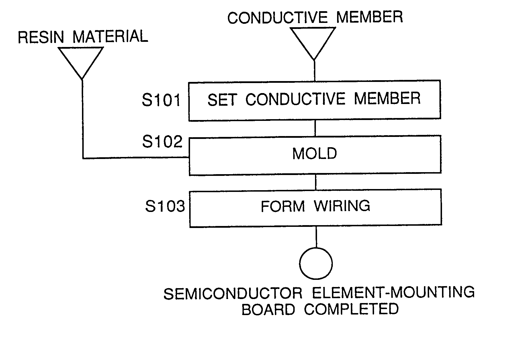
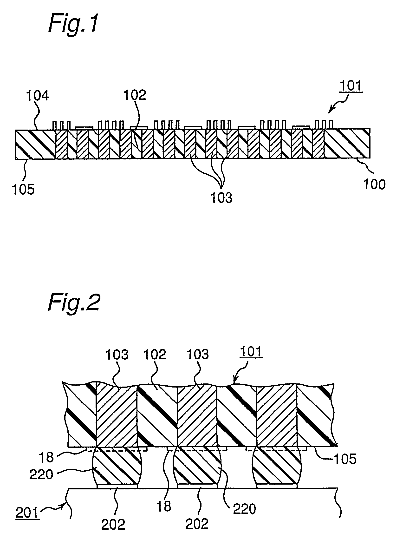
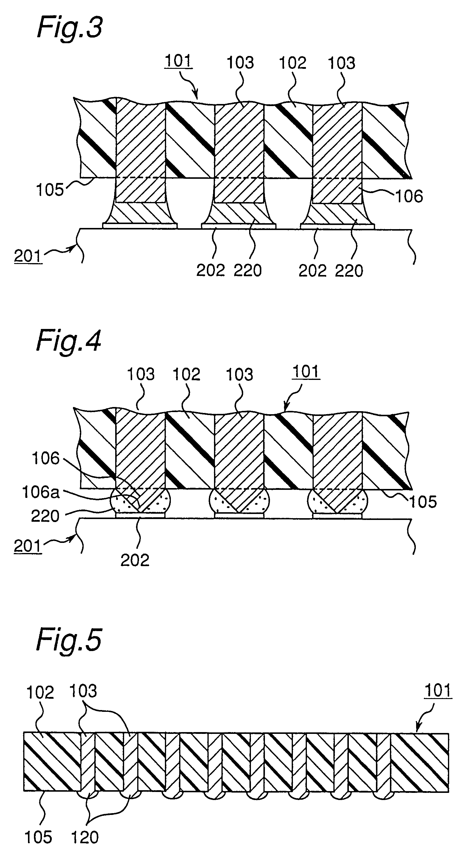
[0070]A semiconductor element-mounting board 101 shown in FIG. 1 is generally called a carrier and corresponds to the semiconductor element-mounting board 2 described with reference to FIG. 21. Roughly speaking, the board 101 comprises a base member 100 including resin material 102 and linear conductive members 103....


PUM


Abstract

A method of manufacturing a semiconductor mounting board includes providing a base member and linear conductive members formed of metallic wires. The conductive members are constructed so that they extend linearly between a semiconductor element-mounting face and a circuit board-mounting face of a base member, and are integrally molded within the base member. For this purpose, a resin material for forming the base member is injected into a mold wherein the conductive members are linearly arranged beforehand.

Description

[0001]This application is a Continuation Application of Ser. No. 09 / 878,419 filed Jun. 12, 2001, now abandoned, which is a Divisional Application of Ser. No. 08 / 890,009, filed Jul. 8, 1997, now U.S. Pat. No. 6,265,673 B1.BACKGROUND OF THE INVENTION[0002]The present invention relates to a semiconductor element-mounting board with a semiconductor mounted thereto by a flip-chip mounting method, and a semiconductor device using the semiconductor element-mounting board.[0003]Along with the current rapid progress changing electronic appliances to be compact and exhibit high-performance, as represented by portable phones, personal computers, pager units, etc., the number of semiconductors used in each electronic circuit has increased. Meanwhile, the electronic circuit comes to use a frequency band as high as 1 GHz, whereby not only the processing speed of an integrated circuit (IC) matters, but the wiring length of the electronic circuit also matters much. The IC is consequently being chan...

Claims


Application Information

Patent Timeline
IPC IPC(8): H01K3/22H01L21/60H01L21/48H01L23/12H01L23/498H01L23/52H05K1/18
CPCH01L21/486H01L23/49827H01L2224/16H01L2924/01046H01L2924/01078H01L2924/01079Y10T29/49156H01L2924/15311H01L2924/01019H01L2224/73204Y10T29/49158Y10T29/49128Y10T29/49146H01L2924/09701H01L24/05H01L2224/05567H01L2224/05573H01L2224/05624H01L2924/00014H01L21/565
Inventor HIGASHIDA, TAKAAKIKUMAGAI, KOICHIMATSUO, TAKAHIRO
Owner PANASONIC CORP
Why Eureka
Try Eureka