Method and device for cutting wire formed on semiconductor substrate

a technology of semiconductor substrate and processing operation, which is applied in the direction of nuclear energy welding apparatus, semiconductor/solid-state device details, manufacturing tools, etc., can solve the problems of increasing the number of processing operations required to cut wires, unsatisfactory short-circuiting, etc., and achieve the effect of preventing such short-circuiting and increasing the number of processing operations

Inactive Publication Date: 2006-05-02
SOCIONEXT INC
View PDF8 Cites 5 Cited by
  • Summary
  • Abstract
  • Description
  • Claims
  • Application Information

AI Technical Summary

Benefits of technology

[0007]However, in recent years, copper is often used as the material of the wire. When cutting copper wires with an FIB device, the stray material is viscous. Thus, the stray material may cause undesirable short-circuiting. Gas assisted etching must be performed to prevent such short-circuiting. However, when cutting wires through gas assisted etching, know-how, such as how to perform gas assisted etching in accordance with the wire thickness, the wire width, and the surrounding conditions of the wire becomes necessary. This increases the number of processing operations required to cut a wire.
[0008]The present invention provides a method and device that ensures the cutting of a wire with a small number of processing operations.
[0010]A further aspect of the present invention is a method for cutting a wire formed on a semiconductor substrate. The method including forming a cut portion by scanning the semiconductor substrate with a focused ion beam to cut the wire, and forming a redundant portion, continuously from the cut portion, for preventing stray material from the wire from being formed continuously with the cut portion.

Problems solved by technology

Thus, the stray material may cause undesirable short-circuiting.
This increases the number of processing operations required to cut a wire.

Method used


Image

  • Method and device for cutting wire formed on semiconductor substrate
  • Method and device for cutting wire formed on semiconductor substrate
  • Method and device for cutting wire formed on semiconductor substrate

Examples


Embodiment Construction

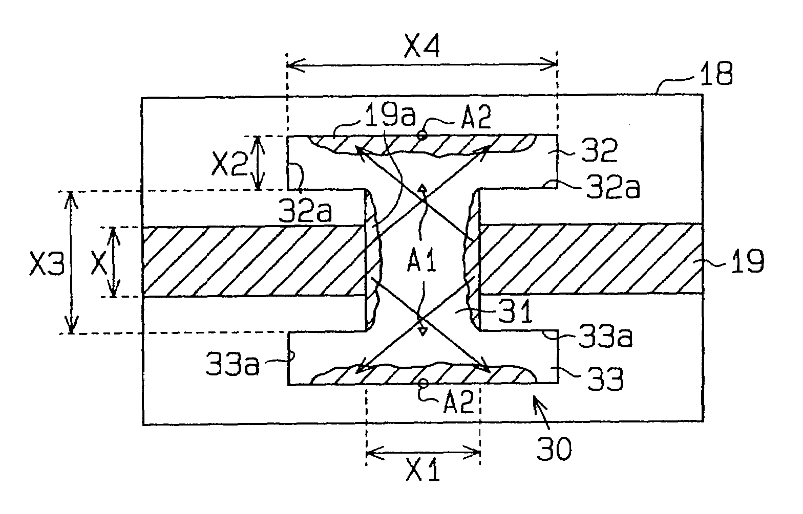
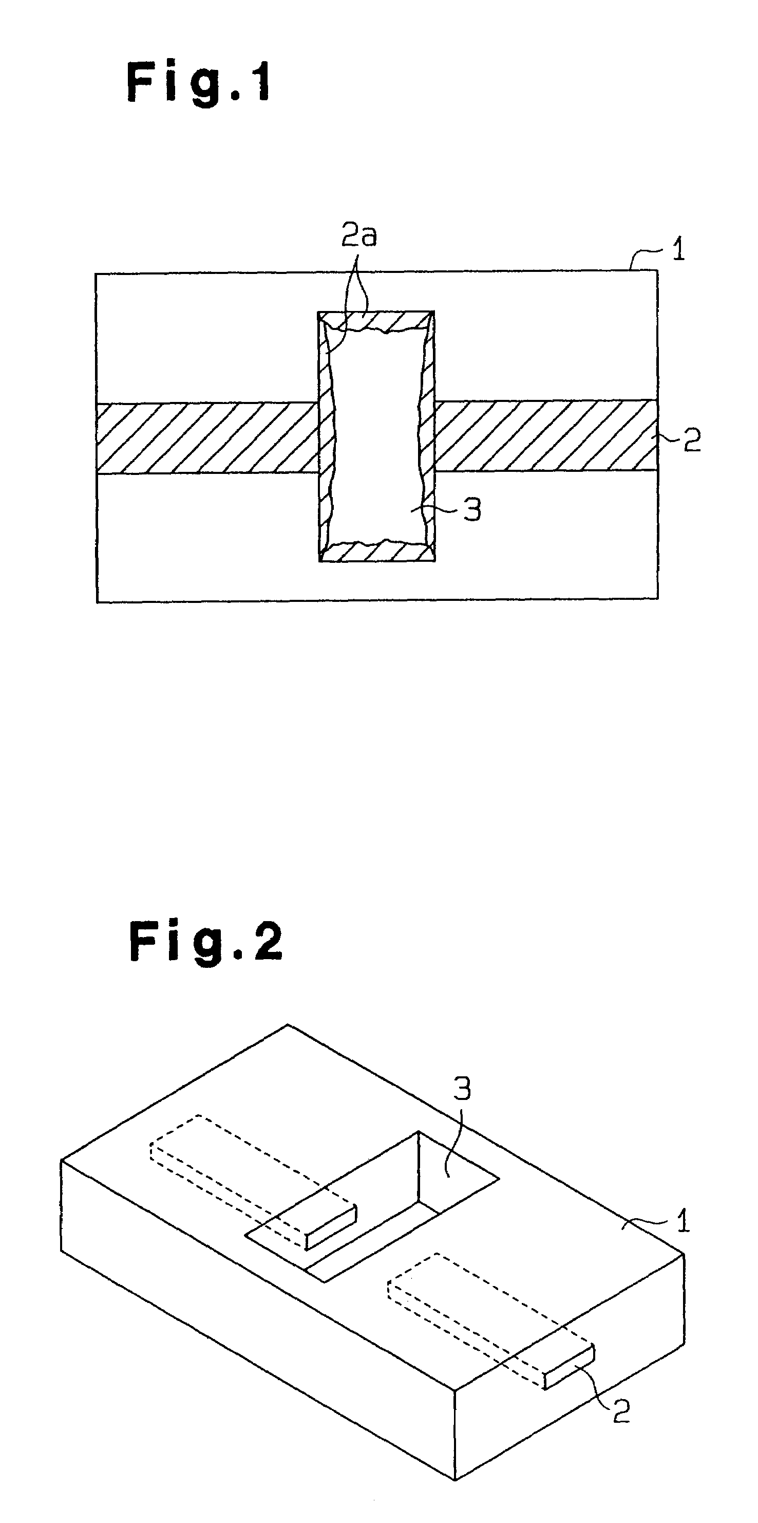
[0026]In the drawings, like numerals are used for like elements throughout.

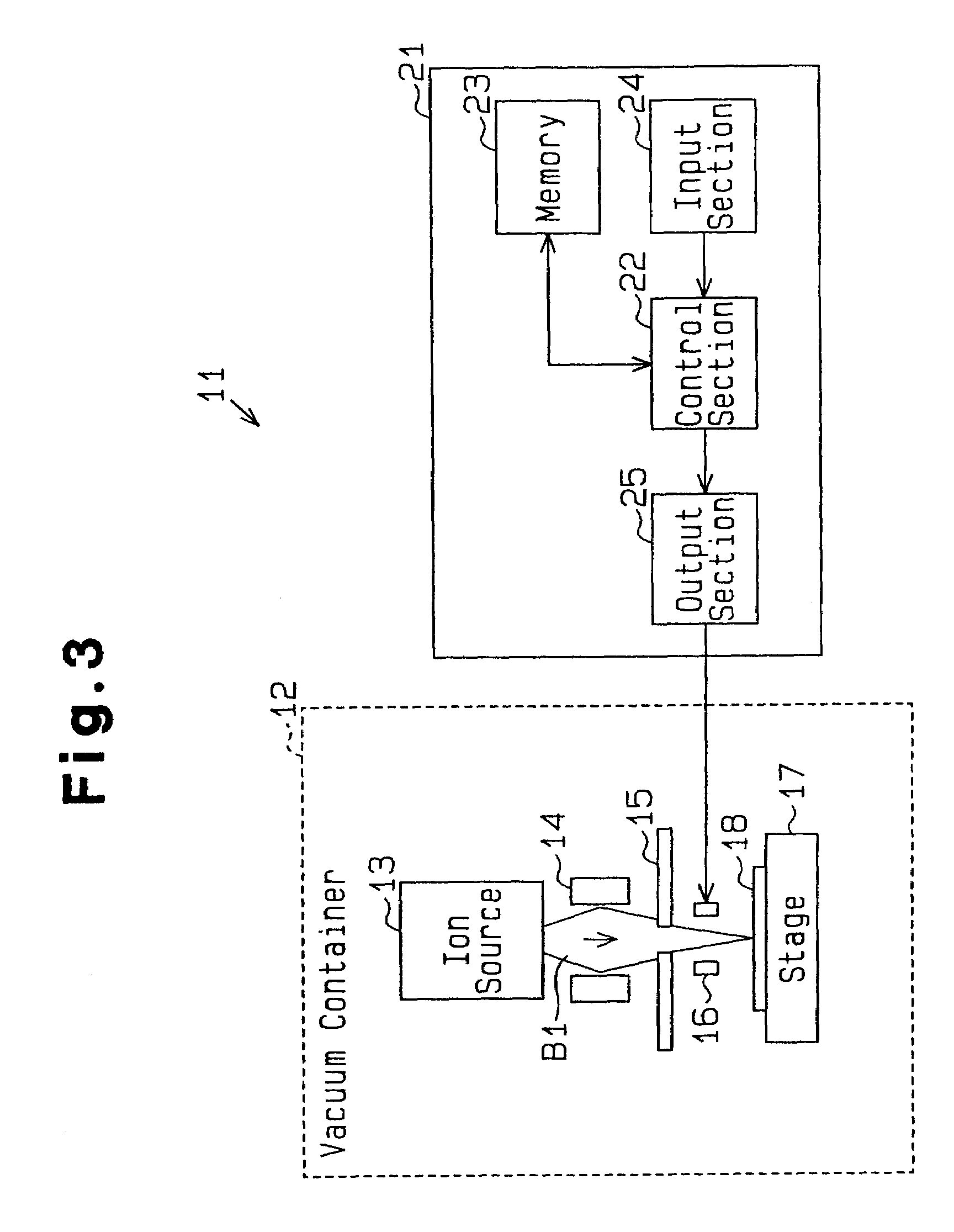
[0027]A method and device according to a preferred embodiment of the present invention will now be discussed with reference to FIGS. 3 to 9.

[0028]FIG. 3 is a schematic block diagram of a focused ion beam processing device (FIB device) 11 that cuts wires formed on a semiconductor substrate 18.

[0029]The FIB device 11 includes a vacuum container 12. The vacuum container 12 accommodates a processor, which includes an ion source 13, an electronic system 14, an aperture 15, a deflector 16, and a stage 17. In the FIB device 11, the ion source 13 emits an ion beam B1. The electronic system 14 applies a predetermined acceleration voltage to the ion beam B1 to focus the ion beam B1. The ion beam B1 is further focused when passing through the aperture 15. Then, the deflector (scanning deflector) 16 deflects the ion beam B1. This emits the ion beam B1 toward a sample (semiconductor substrate 18 on which a wire subject to...


PUM

PropertyMeasurementUnit
semiconductoraaaaaaaaaa
volatileaaaaaaaaaa
thicknessaaaaaaaaaa

Abstract

Method and device for cutting a wire with a small number of processing operations. The method includes forming a cut portion by scanning the semiconductor substrate with a focused ion beam to cut the wire. The method further includes forming a clear region continuously from the cut portion by scanning the semiconductor substrate with the focused ion beam. The clear region is free of stray material of the wire.

Description

CROSS REFERENCE TO RELATED APPLICATIONS[0001]This application is based upon and claims the benefit of priority from the prior Japanese Patent Application No. 2003-361072, filed on Oct. 21, 2003, the entire contents of which are incorporated herein by reference.BACKGROUND OF THE INVENTION[0002]The present invention relates to a method and apparatus for cutting a wire formed on a semiconductor substrate by scanning the wire with a focused ion beam.[0003]Semiconductor integrated circuits (e.g., LSI) have become highly integrated and provided with higher functions over recent years. When developing an LSI, logic for many circuits must be corrected. More specifically, when a circuit does not function due to a logic error or a layout error, a focused ion beam process is performed to cut a wire at the location where the error occurred. There is a demand for technology that ensures the cutting of the wire with a focused ion beam.[0004]A device (FIB device) for cutting a wire that is formed ...

Claims


Application Information

Patent Timeline
Patent Type & Authority Patents(United States)
IPC IPC(8): H01L21/00B23K17/00H01L21/302C23F4/00H01L21/3205H01L21/768H01L21/82H01L23/52
CPCB23K17/00H01L21/76894Y10S438/961H01L21/82
Inventor MARUTA, YUKIOMIZUNO, KINICHI
Owner SOCIONEXT INC
Why Eureka
Try Eureka