Method of manufacturing flash memory device

Inactive Publication Date: 2006-05-02
SK HYNIX INC
View PDF5 Cites 26 Cited by
  • Summary
  • Abstract
  • Description
  • Claims
  • Application Information

AI Technical Summary

Benefits of technology

[0009]One disclosed method of manufacturing flash memory device is capable of sufficiently reducing the critical dimension of the active re

Problems solved by technology

Accordingly, the disclosed methods for manufacturing flash memory devices substantiall

Method used


Image

  • Method of manufacturing flash memory device
  • Method of manufacturing flash memory device
  • Method of manufacturing flash memory device

Examples


Embodiment Construction

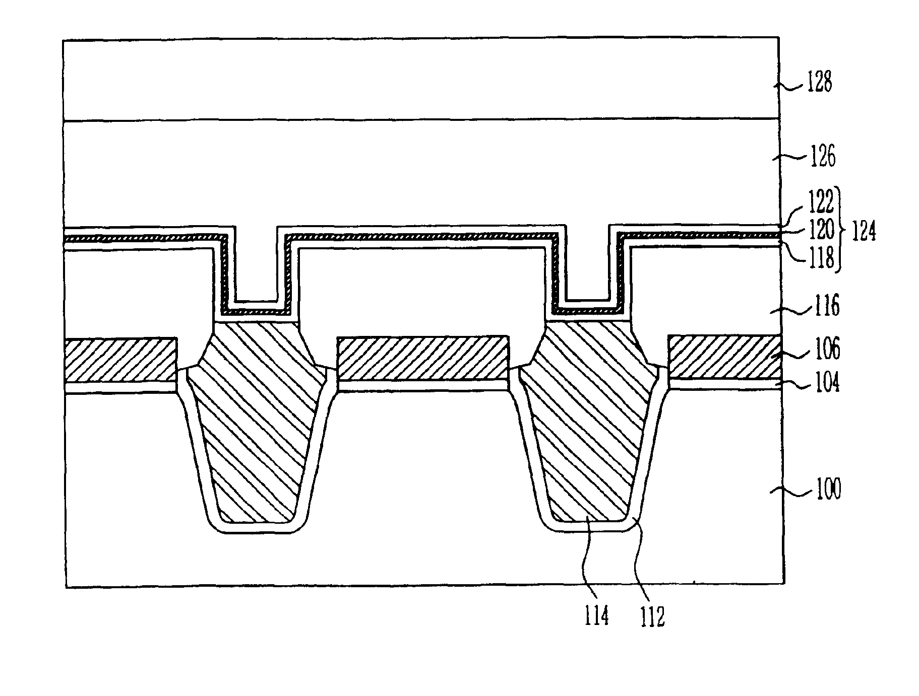
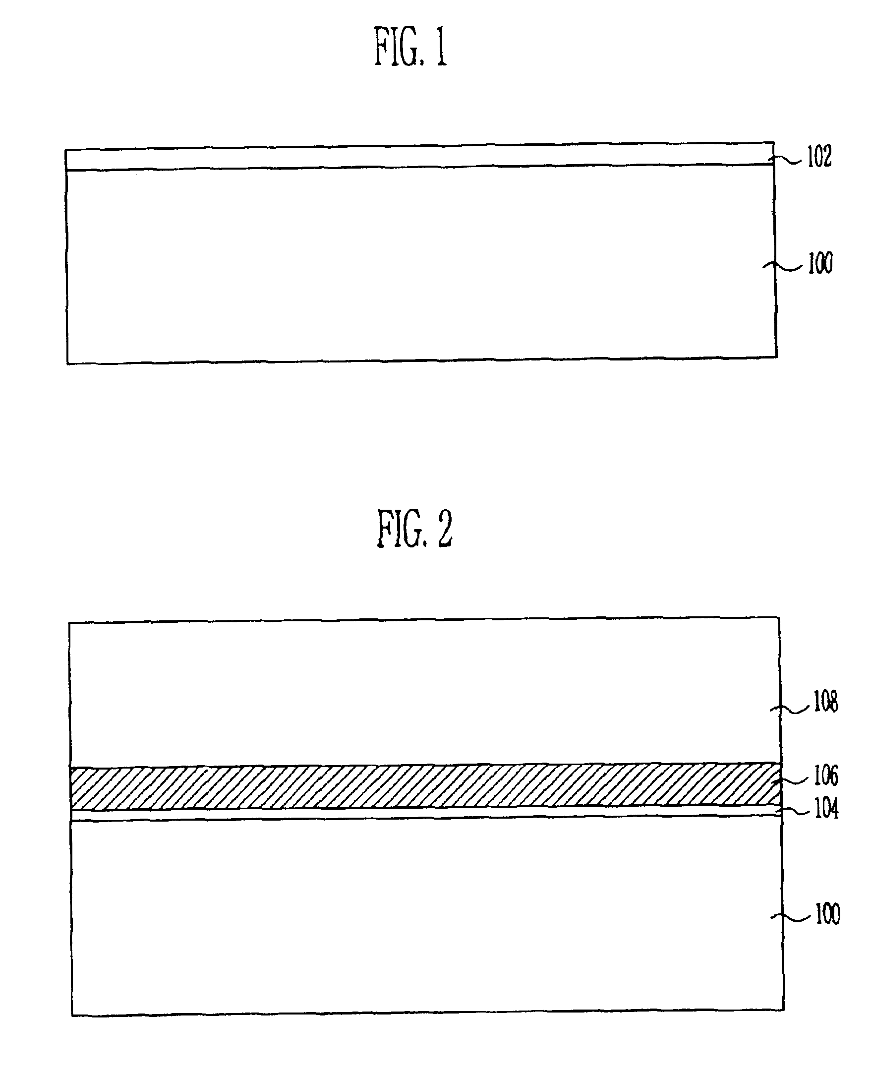
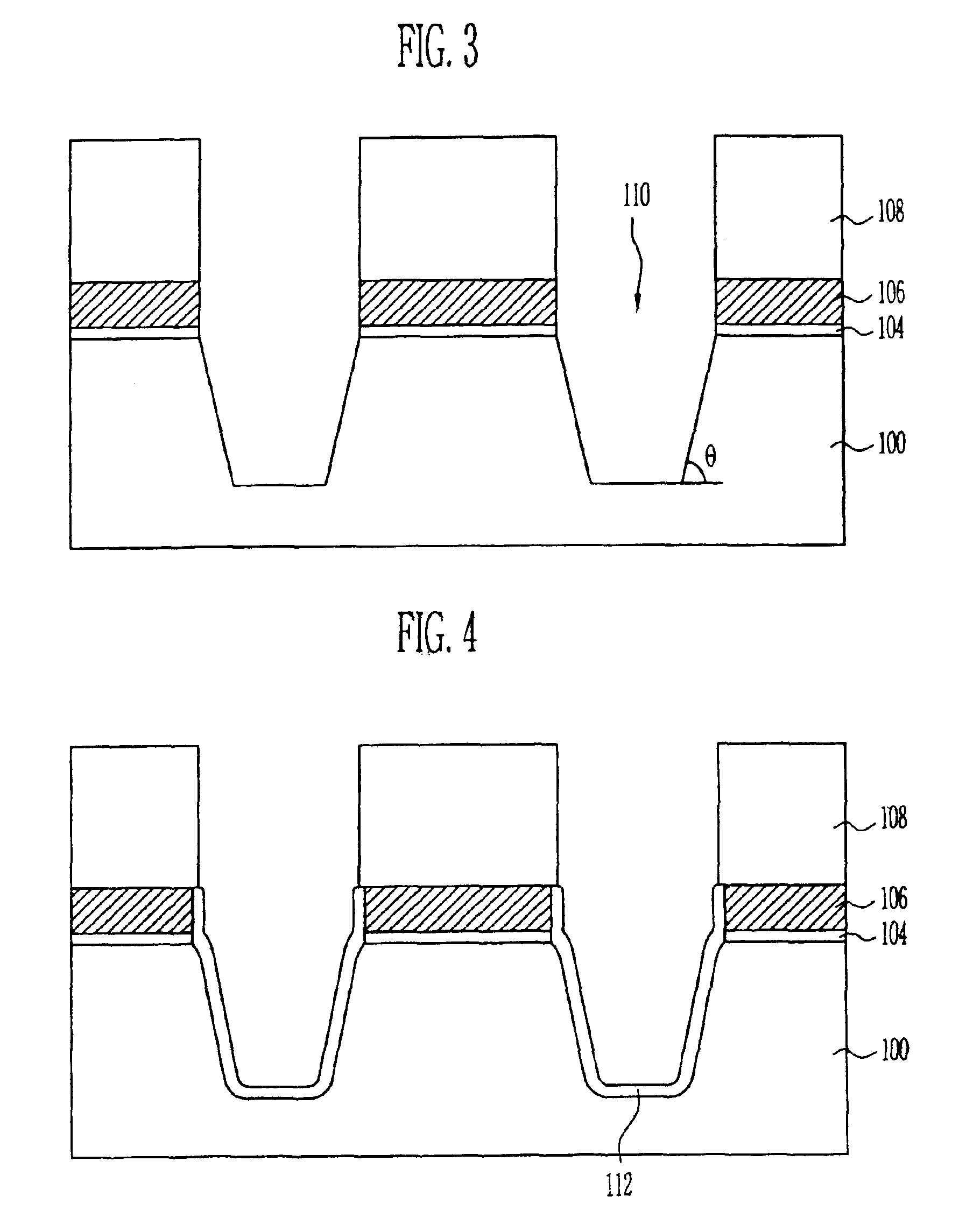
[0014]Reference will now be made in detail to the preferred embodiments, the disclosed examples of which are illustrated in the accompanying drawings, in which like reference numerals are used to identify the same or similar parts. FIG. 1˜FIG. 11 are cross-sectional views of flash memory devices for explaining the disclosed methods for manufacturing flash memory devices.

[0015]Referring to FIG. 1, a semiconductor substrate 100 the top surface of which is cleaned through a pre-treatment cleaning process is prepared. At this time, it is preferable that the pre-treatment cleaning process is implemented using DHF (diluted HF; solution where H2O is mixed in a given ratio) and SC-1(standard cleaning-1; solution where NH4OH / H2O2 / H2O solutions are mixed in a given ratio), or BOE (buffer oxide etchant; solution where HF / NH4F / H2O solutions are mixed in a given ratio) and SC-1.

[0016]For the purpose of prohibiting crystal defects on the top surface of the semiconductor substrate 100 or surface p...


PUM


Abstract

Disclosed is a method of manufacturing the flash memory device. The method comprises the steps of sequentially forming a tunnel oxide film, a first polysilicon film and a hard mask film on a semiconductor substrate, etching portions of the hard mask film, the first polysilicon film, the tunnel oxide film and the semiconductor substrate through a patterning process to form a trench within the semiconductor substrate, depositing an oxide film to bury the trench and then polishing the oxide film by means of a chemical mechanical polishing process until the hard mask film is exposed, removing the hard mask film, implementing a cleaning process so that a protrusion of the oxide film is recessed to an extent that the sidewall bottom of the first polysilicon film is not exposed, depositing a second polysilicon film on the results in which the protrusion of the oxide film is recessed and then polishing the second polysilicon film until the protrusion of the oxide film is exposed, forming a dielectric film on the second polysilicon film, and forming a control gate on the dielectric film.

Description

BACKGROUND[0001]1. Technical Field[0002]Methods of manufacturing flash memory devices are disclosed.[0003]2. Background of the Related Art[0004]In implementing the flash memory devices, shallow trench isolation (hereinafter called ‘STI’) is employed. In the prior art, as the sidewall oxidization process is employed, a tunnel oxide film formed at the top corner of the trench is formed in thickness thinner than a deposition target. The thickness of the tunnel oxide film formed at the top corner of the trench becomes thinner than that of the tunnel oxide film formed at its center. Furthermore, in order to sufficiently reduce the critical dimension (hereinafter called ‘CD’) in the active region, a photolithography technology of a micro line width is required. For this, expensive equipments are required and the cost price is thus increased. In addition, there are limitations in increasing the surface area of the floating gate and the capacitance value applied to the ONO (oxide / nitride / ox...

Claims


Application Information

Patent Timeline
IPC IPC(8): H01L21/336H01L21/762H01L21/8247H01L27/115H01L29/788H01L29/792
CPCH01L21/76232H01L27/11521H01L27/115H10B69/00H10B41/30
Inventor DONG, CHA DEOKSON, HO MIN
Owner SK HYNIX INC
Why Eureka
Try Eureka