Bipolar transistor structure with self-aligned raised extrinsic base and methods

a raised extrinsic base, bipolar transistor technology, applied in the direction of basic electric elements, electrical apparatus, semiconductor devices, etc., can solve the problems of poor rb control, increased process complexity, increased rb but, etc., to eliminate complexity and cost

Active Publication Date: 2006-05-02
INT BUSINESS MASCH CORP
View PDF21 Cites 27 Cited by
  • Summary
  • Abstract
  • Description
  • Claims
  • Application Information

AI Technical Summary

Benefits of technology

[0015]In one embodiment, the invention includes a method of fabricating a bipolar transistor structure that provides fT and fMAx improvements of a raised extrinsic base using non-self-aligned techniques to establish a self-aligned structure. Accordingly, the invention eliminates the complexity and cost of current self-aligned raised extrinsic base processes. The invention forms a raised extrinsic base and an emitter opening over a landing pad, i.e., etch stop layer, then replaces the landing pad with a conductor that is converted, in part, to an insulator. An emitter is then formed in the emitter opening once the insulator is removed from the emitter opening. An unconverted portion of the conductor provides a conductive base link and a remaining portion of the insulator under a spacer isolates the extrinsic base from the emitter while maintaining self-alignment of the emitter to the extrinsic base. The invention also includes the resulting bipolar transistor structure.
[0019]In other embodiments, the invention includes methods of fabricating a bipolar transistor that adds a silicon germanium (SiGe) layer or a third insulator layer of, e.g., high pressure oxide (HIPOX), atop an emitter cap on top of the intrinsic base prior to forming a link-up layer. This addition allows for removal of the link-up layer using wet etch chemistries to remove the excess SiGe or third insulator layer formed atop the emitter cap without using oxidation. In this case, an oxide section (formed by deposition of an oxide or segregation of the above-mentioned HIPOX layer) and nitride spacer can be used to form the emitter-base isolation. The invention results in lower thermal cycle, lower stress levels, and more control over the emitter cap layer thickness, which are drawbacks of the first embodiment. The invention also includes the resulting bipolar transistor structure.

Problems solved by technology

Current approaches to achieve these improvements increase process complexity in order to maintain the extrinsic base self-aligned to the emitter, or employ a non-self aligned (NSA) structure in favor of a more simple process.
However, the Chantre et al. process results in less lateral control and higher base resistance due to continuous oxide layer 20, which leads to not only increased Rb but also poorer Rb control.
However, this process is complex.
Another challenge to improving ICs fabricated for high performance mixed signal applications is that performance of self-aligned bipolar transistors with extrinsic base degrades as the emitter dimension is reduced due to loss of intrinsic base definition caused by the lateral diffusion of dopants.
In this approach, an extrinsic base of area A and depth D is constructed to have a low aspect ratio (D / A <<1), which can lead to a significant difference in the extrinsic base layer thickness between the small and large devices, and isolated and nested devices, due to dishing caused by the CMP.
Unfortunately, special techniques are required to ensure a good link-up contact between the intrinsic base and the extrinsic base.
One drawback of this approach is that the epitaxial growth to form the link-up also forms a silicon layer over the emitter cap layer at the bottom of the opening.
As a result, the silicon layer needs to be oxidized to consume the excess silicon.
The oxidation of the excess silicon layer is detrimental in a number of ways.
First, it causes widening of the base profile, which reduces fT.
Second, it causes non-uniform emitter cap thickness because it is difficult to control the depth of penetration of the oxidation.
This situation results in widespread transistor current gain, Icollector / Ibase.
Other approaches to achieve these improvements increase process complexity in order to maintain the extrinsic base self-aligned to the emitter, or employ a non-self aligned (NSA) structure in favor of a more simple process.

Method used


Image

  • Bipolar transistor structure with self-aligned raised extrinsic base and methods
  • Bipolar transistor structure with self-aligned raised extrinsic base and methods
  • Bipolar transistor structure with self-aligned raised extrinsic base and methods

Examples


first embodiment

1. First Embodiment

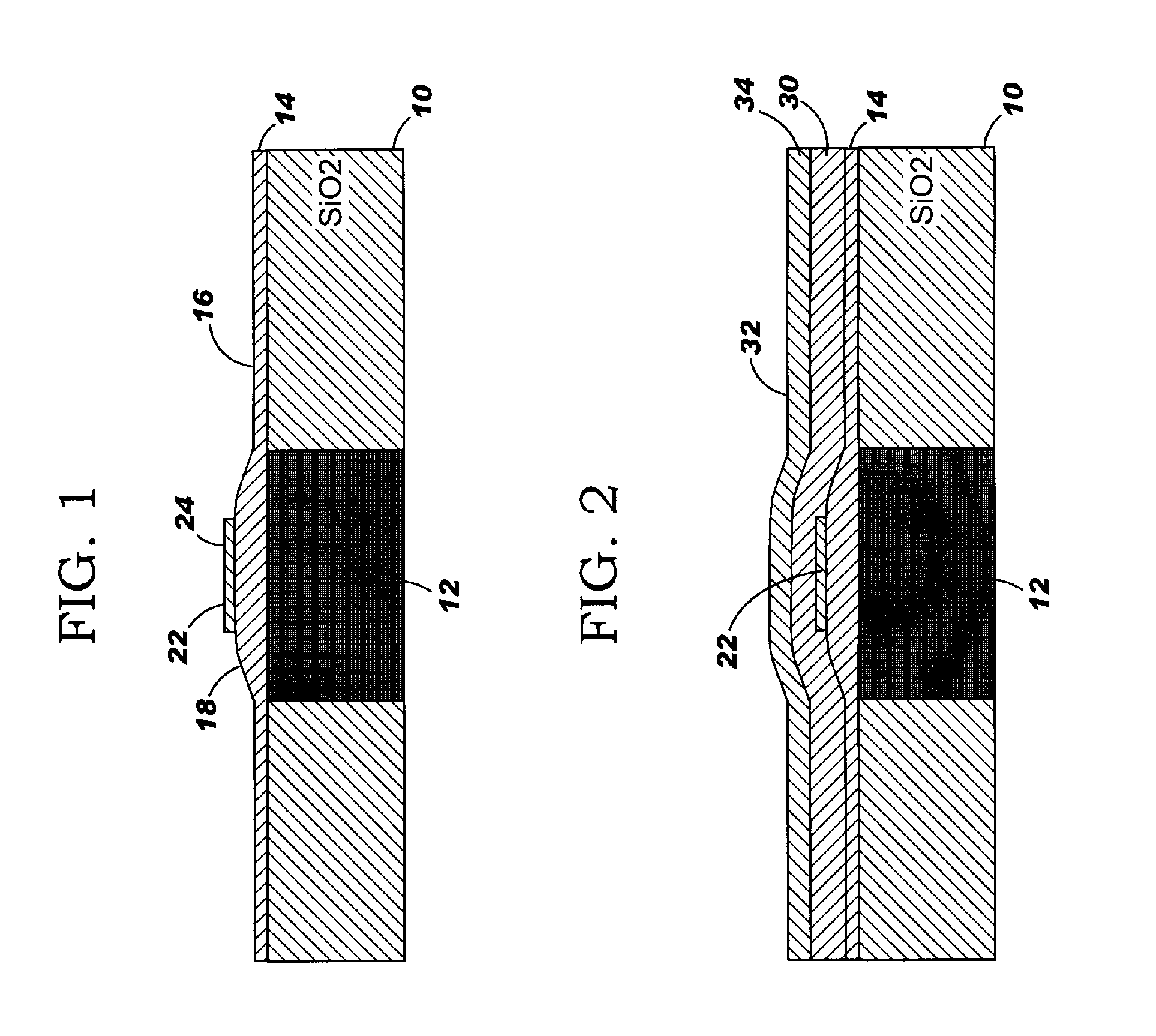
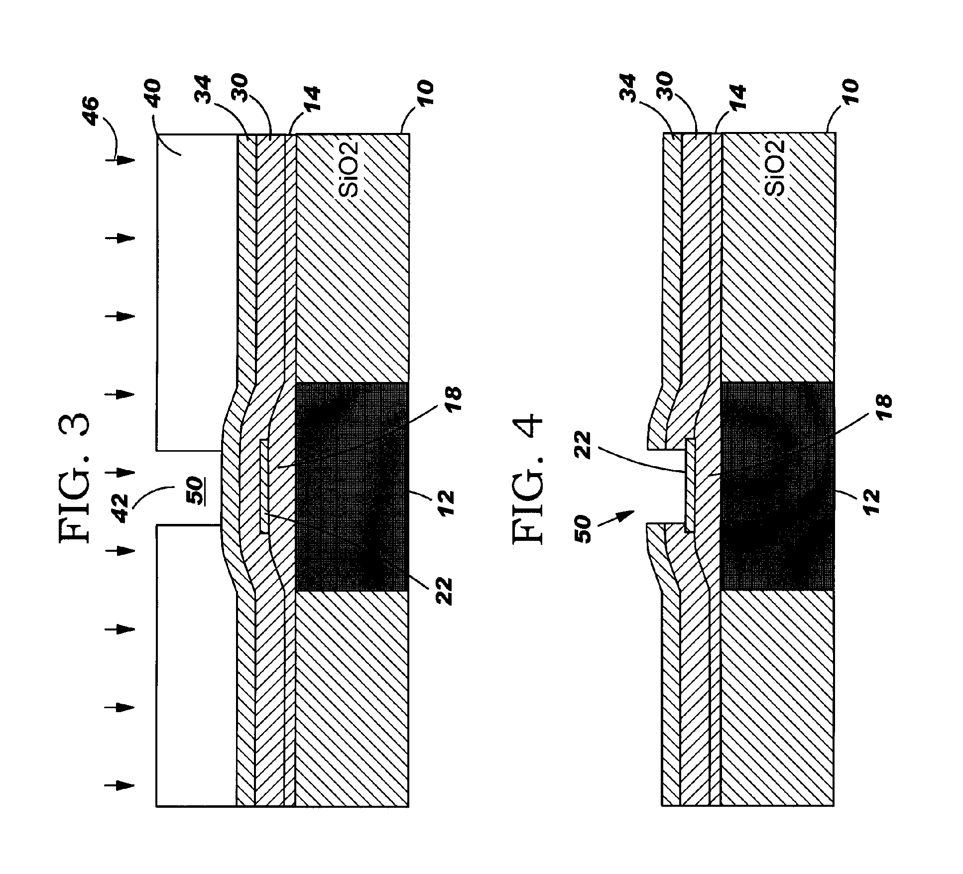
[0051]With reference to the accompanying drawings, FIGS. 1–10 illustrate a first embodiment of the invention. FIG. 1 shows a starting point for the processing of the invention according to the first embodiment. In FIG. 1, a shallow-trench isolation (STI) 10 is provided of silicon dioxide (SiO2) (hereinafter “oxide”) having an active silicon (Si) region 12 in a portion thereof. A low temperature epitaxial (LTE) growth of silicon over this structure results in an intrinsic base layer 14 including a polysilicon portion 16 formed over STI 10 and a silicon intrinsic base portion 18 formed over active silicon region 12. Intrinsic base portion 18, as will become apparent below, provides an intrinsic base of a resulting self-aligned bipolar transistor structure 200 (FIG. 10).

[0052]A first insulator layer (not shown in its entirety) is then formed over intrinsic base layer 14, patterned and etched to form a landing pad 22, i.e., an etch stop layer, on a portion 24 of intri...

second embodiment

2. Second Embodiment

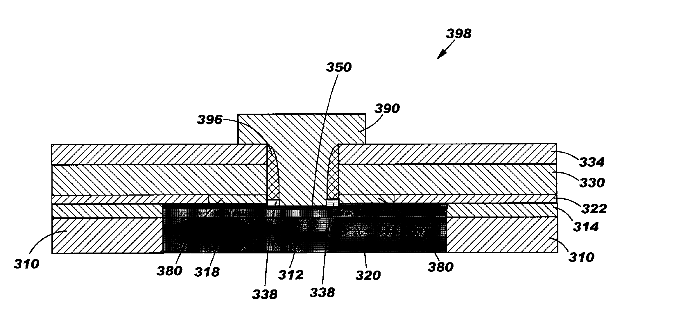
[0061]Referring to FIGS. 11–18, a second embodiment of the invention will now be described. FIG. 11 illustrates a starting point for the processing of the invention according to the second embodiment. In FIG. 11, a structure 300 is provided including a polycrystalline intrinsic base layer 314, an intrinsic base 320 and an emitter cap 318 adjacent polycrystalline intrinsic base layer 314, a first insulator layer 322 on emitter cap 318, a raised extrinsic base layer 330 over first insulator layer 322, and a second insulator layer 334 over raised extrinsic base layer 330. Emitter cap 318 and intrinsic base 320 are provided over an active silicon region 312. Emitter cap 318 may be formed by a low temperature epitaxial silicon growth over a silicon-germanium containing layer of intrinsic base 320, which is over active silicon region 312. Polycrystalline intrinsic base layer 314 is adjacent to emitter cap 318 and intrinsic base 320. Polycrystalline intrinsic base layer...

third embodiment

3. Third Embodiment

[0068]Referring to FIGS. 19–26, a third embodiment of the invention will now be described. FIG. 19 illustrates a starting point for the processing of the invention according to the second embodiment. In FIG. 19, a structure 400 is provided including a polycrystalline intrinsic base layer 414 including an intrinsic base 420, an emitter cap 418, and a thin silicon-germanium (SiGe) etch-stop layer 417 over emitter cap 418. Provision of emitter cap 418, SiGe etch-stop layer 417 and intrinsic base 420, which may include SiGe, may be formed by a conventional low temperature selective or non-selective epitaxial growth. Polycrystalline intrinsic base layer 414 is adjacent to intrinsic base 420, emitter cap 418 and etch-stop layer 417, and is deposited over STI 410 of, for example, silicon dioxide. Over polysilicon intrinsic base layer 414 and SiGe etch-stop layer 417 is provided a first insulator layer 422, a raised extrinsic base layer 430 over first insulator layer 422,...


PUM


Abstract

The invention includes methods of fabricating a bipolar transistor that adds a silicon germanium (SiGe) layer or a third insulator layer of, e.g., high pressure oxide (HIPOX), atop an emitter cap adjacent the intrinsic base prior to forming a link-up layer. This addition allows for removal of the link-up layer using wet etch chemistries to remove the excess SiGe or third insulator layer formed atop the emitter cap without using oxidation. In this case, an oxide section (formed by deposition of an oxide or segregation of the above-mentioned HIPOX layer) and nitride spacer can be used to form the emitter-base isolation. The invention results in lower thermal cycle, lower stress levels, and more control over the emitter cap layer thickness, which are drawbacks of the first embodiment. The invention also includes the resulting bipolar transistor structure.

Description

RELATED APPLICATION[0001]This application is a continuation-in-part of application Ser. No. 10 / 707,756, filed Jan. 9, 2004 now U.S. Pat. No. 6,869,852.STATEMENT REGARDING FEDERALLY SPONSORED RESEARCH OR DEVELOPMENT[0002]The subject matter of the present application was at least partially funded under Defense Advanced Research Projects Agency (DARPA) Contract No. N66001-02-C-8014.BACKGROUND OF THE INVENTION[0003]1. Technical Field[0004]The present invention relates generally to bipolar transistors, and more particularly, to a bipolar transistor structure with a self-aligned raised extrinsic base and method of fabricating the same.[0005]2. Related Art[0006]Self-aligned bipolar transistors with raised extrinsic base are the focus of integrated circuits fabricated for high performance mixed signal applications. Producing bipolar transistors for high speed applications requires improvements to the NPN junction to improve unit current gain frequency (fT) and maximum oscillation frequency ...

Claims


Application Information

Patent Timeline
Patent Type & Authority Patents(United States)
IPC IPC(8): H01L21/331H01L29/10
CPCH01L29/1004H01L29/7378H01L29/66287H01L29/66242
Inventor ADAM, THOMAS N.CHAN, KEVIN K.JOSEPH, ALVIN J.KHATER, MARWAN H.LIU, QIZHIRAINEY, BETH ANNSCHONENBERG, KATHRYN T.
Owner INT BUSINESS MASCH CORP
Why Eureka
Try Eureka