Non-volatile memory device capable of changing increment of program voltage according to mode of operation

a non-volatile memory and mode of operation technology, applied in static storage, digital storage, instruments, etc., can solve the problem of difficulty in shortening the time taken during the test program operation, and achieve the effect of shortening the test tim

Active Publication Date: 2006-05-02
SAMSUNG ELECTRONICS CO LTD
View PDF6 Cites 36 Cited by
  • Summary
  • Abstract
  • Description
  • Claims
  • Application Information

AI Technical Summary

Benefits of technology

[0007]It is therefore an object of the invention to provide a non-volatile memory device capable of shortening the test time.

Problems solved by technology

Thus it is difficult to shorten the time taken during the test program operation.

Method used


Image

  • Non-volatile memory device capable of changing increment of program voltage according to mode of operation
  • Non-volatile memory device capable of changing increment of program voltage according to mode of operation
  • Non-volatile memory device capable of changing increment of program voltage according to mode of operation

Examples


Embodiment Construction

[0028]The preferred embodiment of the invention will be more fully described with reference to the attached drawings.

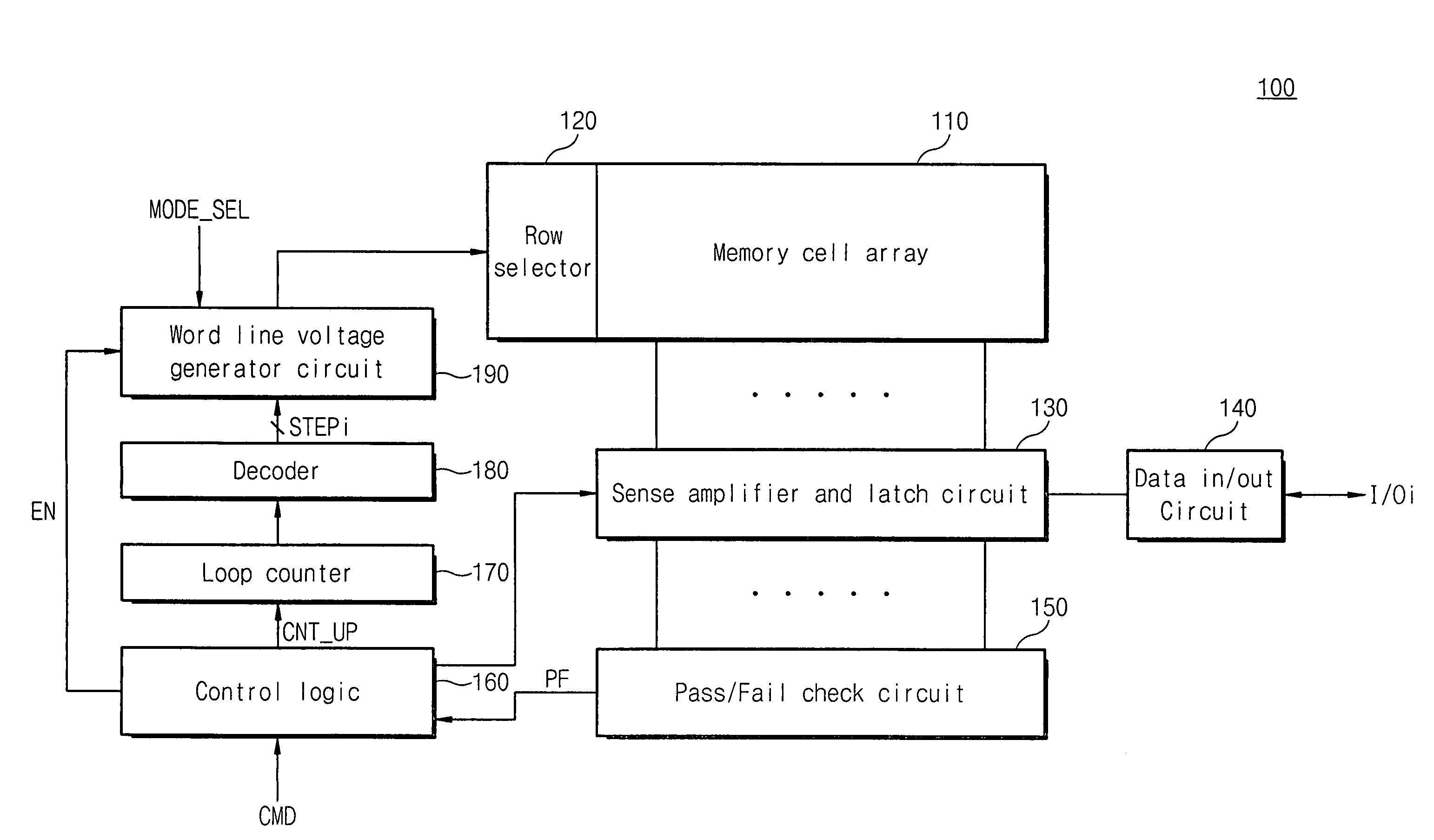
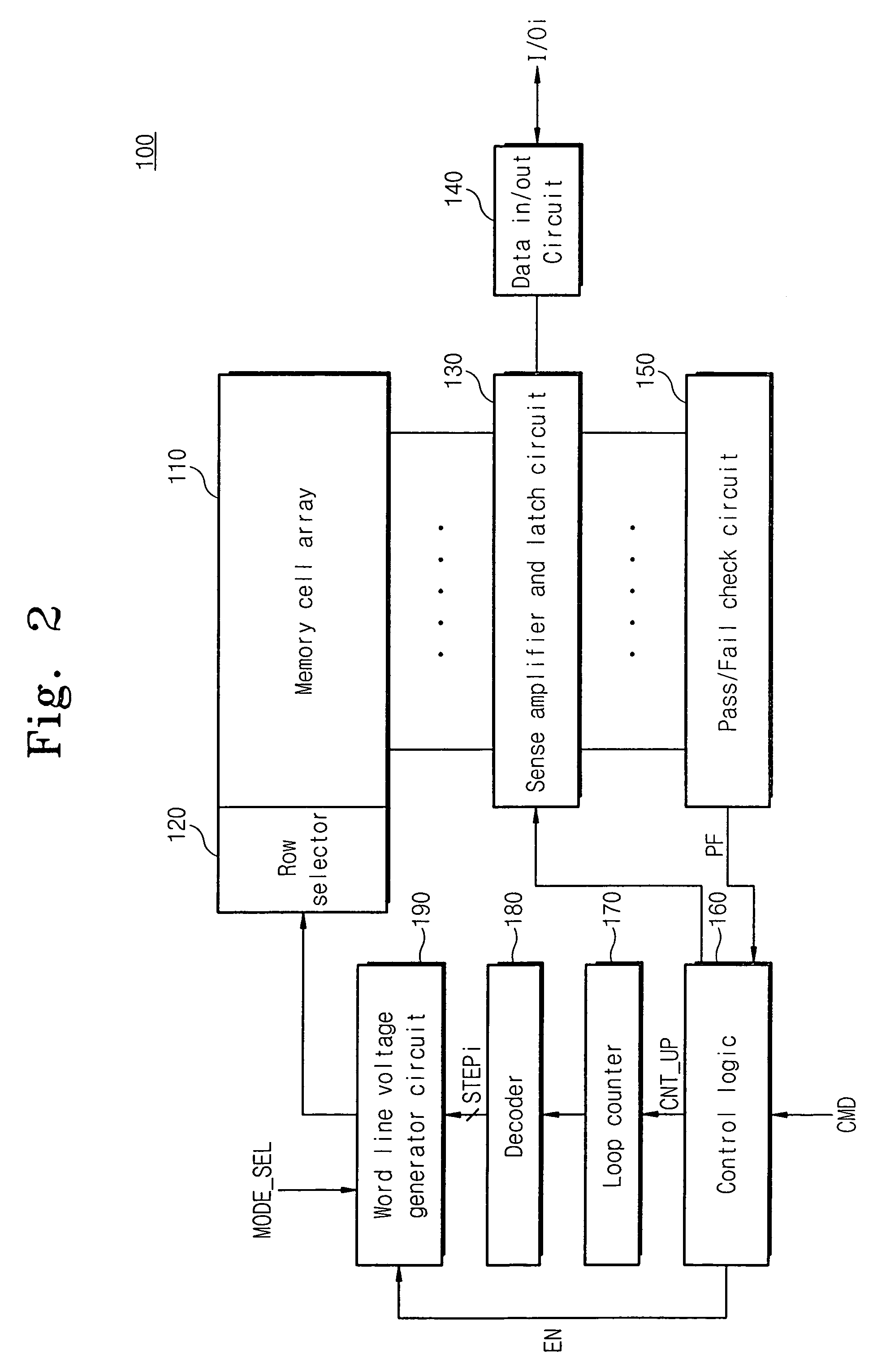
[0029]FIG. 2 schematically shows a non-volatile memory device according to the present invention. A non-volatile memory device 100 according to the present invention is a flash memory device. However, it is obvious to ones skilled in the art that the present invention can be applied to other memory devices (e.g., MROM, PROM, FRAM, etc.).

[0030]The non-volatile memory device 100 of the present invention includes a memory cell array 110 that has memory cells arranged in rows (or word lines) and columns (or bit lines). Each of the memory cells stores 1-bit data. Alternatively, each of the memory cells stores n-bit data (n is an integer greater than 1). A row selector circuit 120 selects at least one of the rows in response to a row address and drives the selected row with a word line voltage from a word line voltage generator circuit 190. A sense amplifier and latch circu...


PUM


Abstract

A non-volatile memory device includes a word line voltage generator circuit for generating a word line voltage to be supplied to a selected row in response to step control signals and a program controller for sequentially activating the step control signals during a program cycle. During the program cycle, the word line voltage generator circuit controls the increment of the word line voltage differently according to the mode of operation, namely, a test mode or a normal mode. Thus test time can be shortened.

Description

CROSS-REFERENCE TO RELATED APPLICATIONS[0001]This U.S. non-provisional patent application claims priority under 35 U.S.C. § 119 of Korean Patent Application 2004-39023 filed on May 31, 2004, the entire contents of which are hereby incorporated by reference.FIELD OF THE INVENTION[0002]The present invention is a semiconductor memory device, and, in particular, a non-volatile memory device.BACKGROUND OF THE INVENTION[0003]In general, semiconductor memory devices are tested in a package and / or wafer level to judge whether defects exit therein. This is accomplished by storing data in memory cells and then reading the stored data from the memory cells. For example, test data is programmed in memory cells of a non-volatile memory device, and then a read operation is performed with a word line voltage varied. As a result of the read operation, this test is capable of measuring a threshold voltage distribution of memory cells. Defects of memory devices, such as a short circuit between cells,...

Claims


Application Information

Patent Timeline
Patent Type & Authority Patents(United States)
IPC IPC(8): G11C16/06G11C16/02G11C11/34G11C16/12G11C16/34G11C29/00G11C29/12
CPCG11C16/12G11C16/3459G11C16/3454
Inventor CHAE, DONG-HYUKBYEON, DAE-SEOK
Owner SAMSUNG ELECTRONICS CO LTD
Why Eureka
Try Eureka