Method for fabricating a high density composite MIM capacitor with reduced voltage dependence in semiconductor dies

Active Publication Date: 2006-05-09
SAMSUNG ELECTRONICS CO LTD
View PDF8 Cites 21 Cited by
  • Summary
  • Abstract
  • Description
  • Claims
  • Application Information

AI Technical Summary

Benefits of technology

[0010]The upper electrode of the lower MIM capacitor is connected to the lower electrode of the upper MIM capacitor while the lower electrode of the lower MIM capacitor is connected to the upper electrode of the upper MIM capacitor; thus forming an embodiment of the invention

Problems solved by technology

Disadvantageously, typical MIM capacitors have low capacitance density and since RF and mixed signal applications require high capacitance values, the die area consumed by typical MIM capacitors is too large, resulting in increased die cost to the manufacturer and the user.
Large voltage coefficients cause an undesirable variation in capacitance.
In a conventional MIM capacitor, when the dielectric thi

Method used


Image

  • Method for fabricating a high density composite MIM capacitor with reduced voltage dependence in semiconductor dies
  • Method for fabricating a high density composite MIM capacitor with reduced voltage dependence in semiconductor dies
  • Method for fabricating a high density composite MIM capacitor with reduced voltage dependence in semiconductor dies

Examples


Embodiment Construction

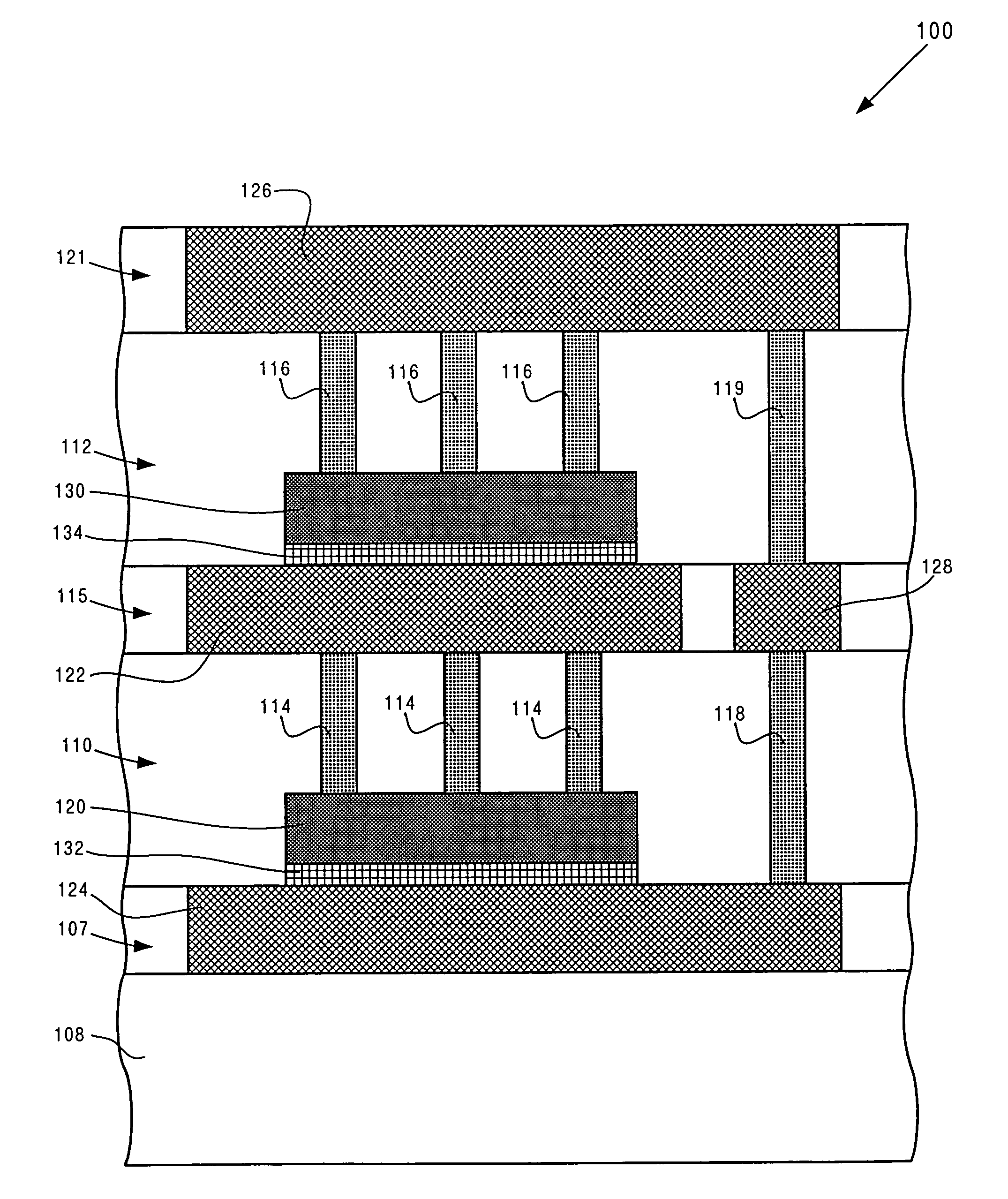
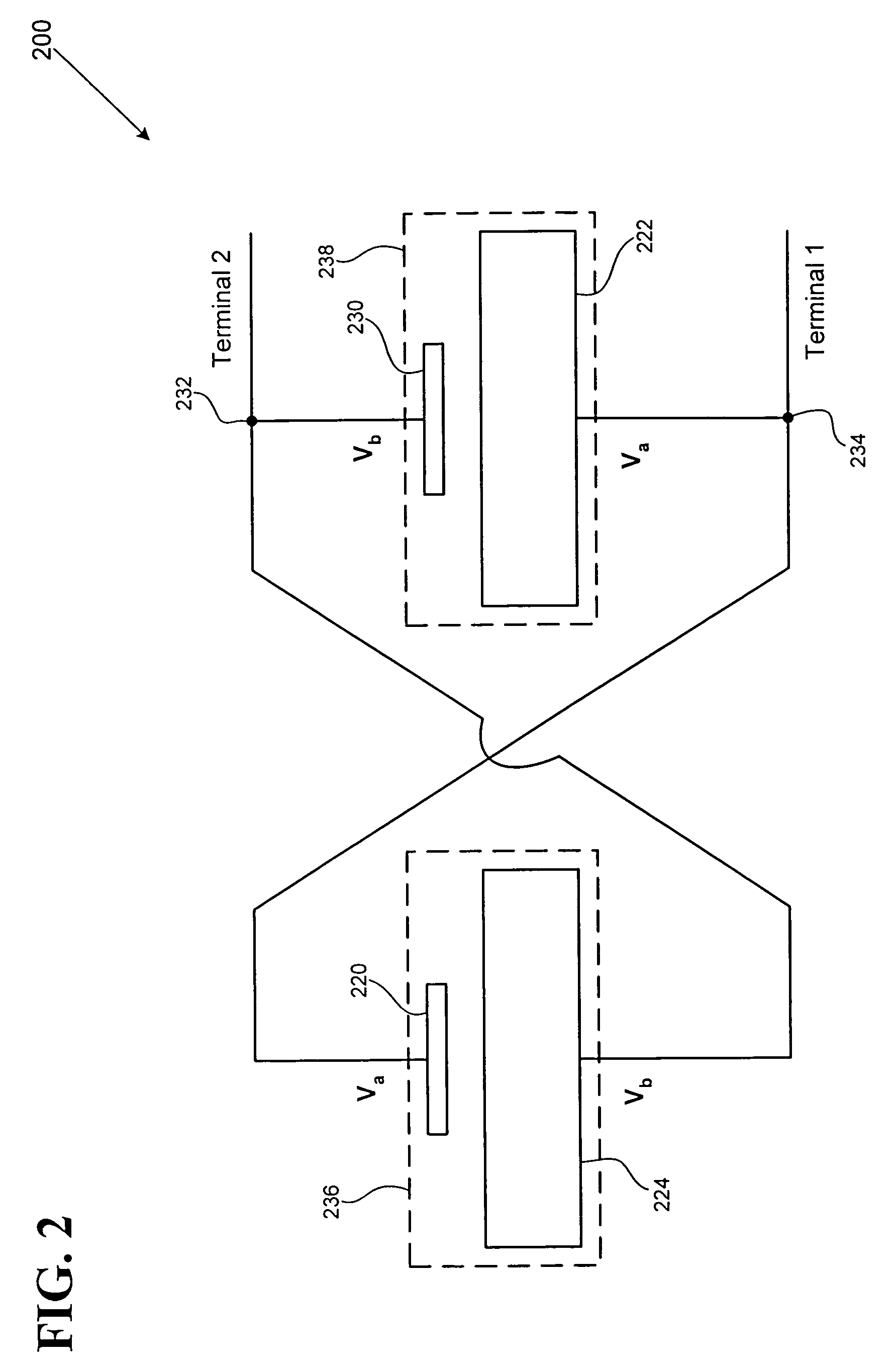
[0014]The present invention is directed to a high density composite MIM capacitor with reduced voltage dependence in semiconductor dies. Although the invention is described with respect to specific embodiments, the principles of the invention, as defined by the claims appended herein, can obviously be applied beyond the specifically described embodiments of the invention described herein. Moreover, in the description of the present invention, certain details have been left out in order to not obscure the inventive aspects of the invention. The details left out are within the knowledge of a person of ordinary skill in the art.

[0015]The drawings in the present application and their accompanying detailed description are directed to merely exemplary embodiments of the invention. To maintain brevity, other embodiments of the invention which use the principles of the present invention are not specifically described in the present application and are not specifically illustrated by the pre...


PUM


Abstract

According to a disclosed embodiment, a composite MIM capacitor comprises a lower electrode of a lower MIM capacitor situated in a lower interconnect metal layer of a semiconductor die. The composite MIM capacitor further comprises an upper electrode of the lower MIM capacitor situated within a lower interlayer dielectric, where the lower interlayer dielectric separates the lower interconnect metal layer from an upper interconnect metal layer. A lower electrode of the upper MIM capacitor is situated in the upper interconnect metal layer. An upper electrode of the upper MIM capacitor is situated within the upper interlayer dielectric which is, in turn, situated over the upper interconnect metal layer. The upper electrode of the lower MIM capacitor is connected to the lower electrode of the upper MIM capacitor while the lower electrode of the lower MIM capacitor is connected to the upper electrode of the upper MIM capacitor.

Description

[0001]This is a divisional of application Ser. No. 10 / 410,937 filed Apr. 9, 2003 now U.S. Pat. No. 6,680,521.BACKGROUND OF THE INVENTION[0002]1. Field of the Invention[0003]The present invention is generally in the field of semiconductor fabrication. More specifically, the invention is in the field of fabrication of capacitors in semiconductor dies.[0004]2. Background Art[0005]High performance mixed signal and RF circuits require high density integrated capacitors. Metal-insulator-metal (“MIM”) capacitors can be considered for use in the fabrication of integrated mixed signal and RF circuits on semiconductor dies. Disadvantageously, typical MIM capacitors have low capacitance density and since RF and mixed signal applications require high capacitance values, the die area consumed by typical MIM capacitors is too large, resulting in increased die cost to the manufacturer and the user.[0006]The capacitance value of a typical MIM capacitor at an applied voltage can be represented by th...

Claims


Application Information

Patent Timeline
IPC IPC(8): H01L21/20H01L21/02H01L21/768H01L27/08
CPCH01L28/40H01L27/0805H01L21/76838H01L27/04
Inventor KAR-ROY, ARJUNRACANELLI, MARCOHOWARD, DAVID
Owner SAMSUNG ELECTRONICS CO LTD
Why Eureka
Try Eureka