Multi-port memory cells for use in FIFO applications that support data transfers between cache and supplemental memory arrays

a memory cell and multi-port technology, applied in the field of multi-port memory cells and memory cell layouts, can solve the problems of data stored therein, data cannot be modified, but only read, and increase the complexity and layout area requirements of these higher bandwidth memory devices

Active Publication Date: 2006-05-09
INTEGRATED DEVICE TECH INC
View PDF99 Cites 38 Cited by
  • Summary
  • Abstract
  • Description
  • Claims
  • Application Information

AI Technical Summary

Problems solved by technology

Because RWM devices use active circuitry to store data, they belong to a class of memory devices known as “volatile” memory devices because data stored therein will be lost upon termination of the power supply.
Since this latter type of data storage may be hardwired, the data cannot be modified, but can only be read.
However, the addition of ports to individual memory cells typically increases the complexity and layout area requirements for these higher bandwidth memory devices.
Unfortunately, a major disadvantage of typical dual-port SRAM-based FIFOs is the relatively large unit cell size for each dual-port SRAM cell therein.
Moreover, the relatively large unit cells of a dual-port SRAM FIFO may limit the degree to which the number of write operations can exceed the number of read operations, that is, limit the capacity of the FIFO.
However, the use of only single port memory cells typically precludes simultaneous read and write access to data in the same memory cell, which means that single-port buffer memory devices typically have slower fall-through time than comparable dual-port memory devices.
Moreover, single-port buffer memory devices may use complicated arbitration hardware to control sequencing and queuing of reading and writing operations.
However, like the above-described single-port buffer memory devices, simultaneous read and write access to data is not feasible.

Method used


Image

  • Multi-port memory cells for use in FIFO applications that support data transfers between cache and supplemental memory arrays
  • Multi-port memory cells for use in FIFO applications that support data transfers between cache and supplemental memory arrays
  • Multi-port memory cells for use in FIFO applications that support data transfers between cache and supplemental memory arrays

Examples


Embodiment Construction

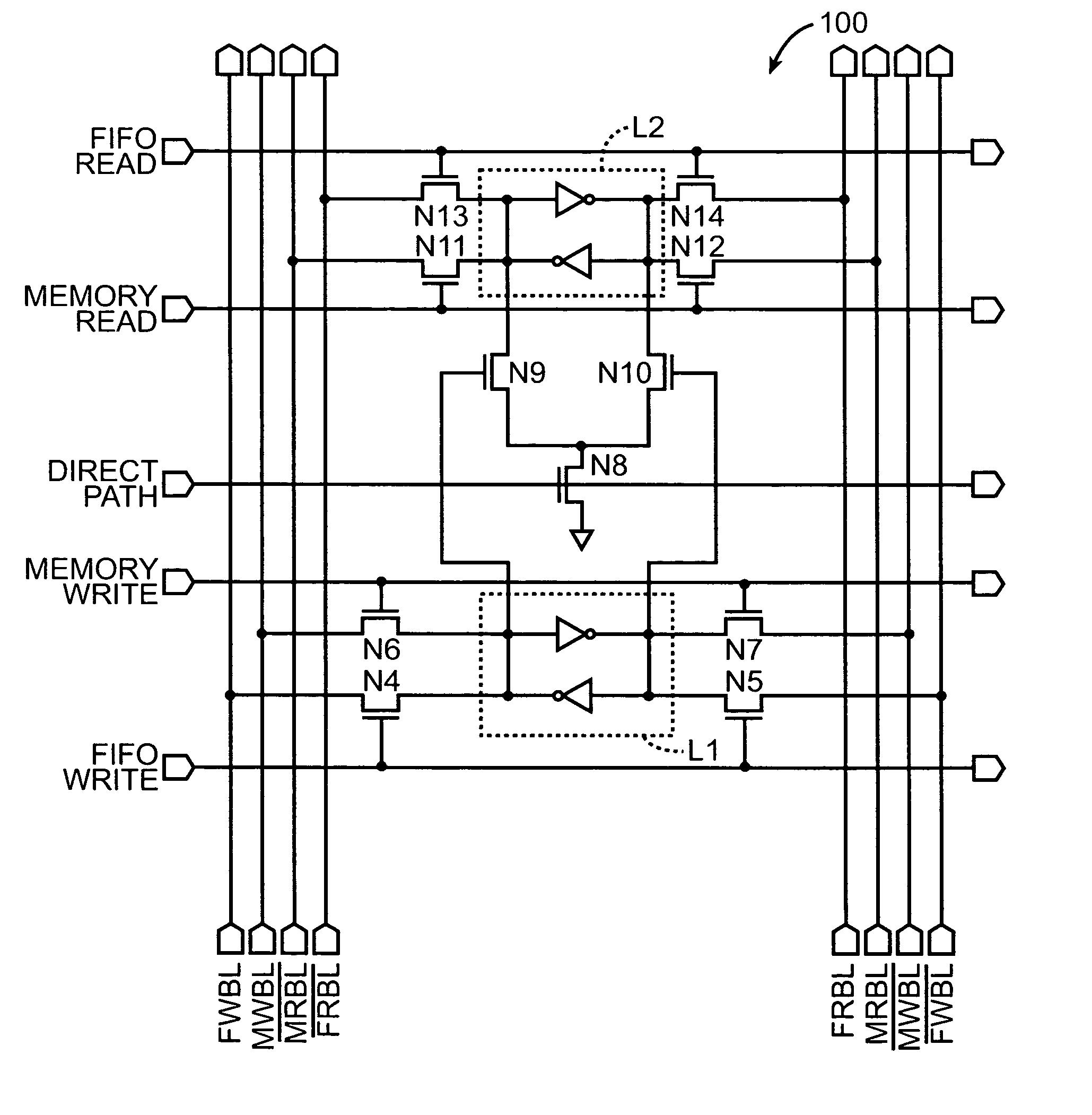
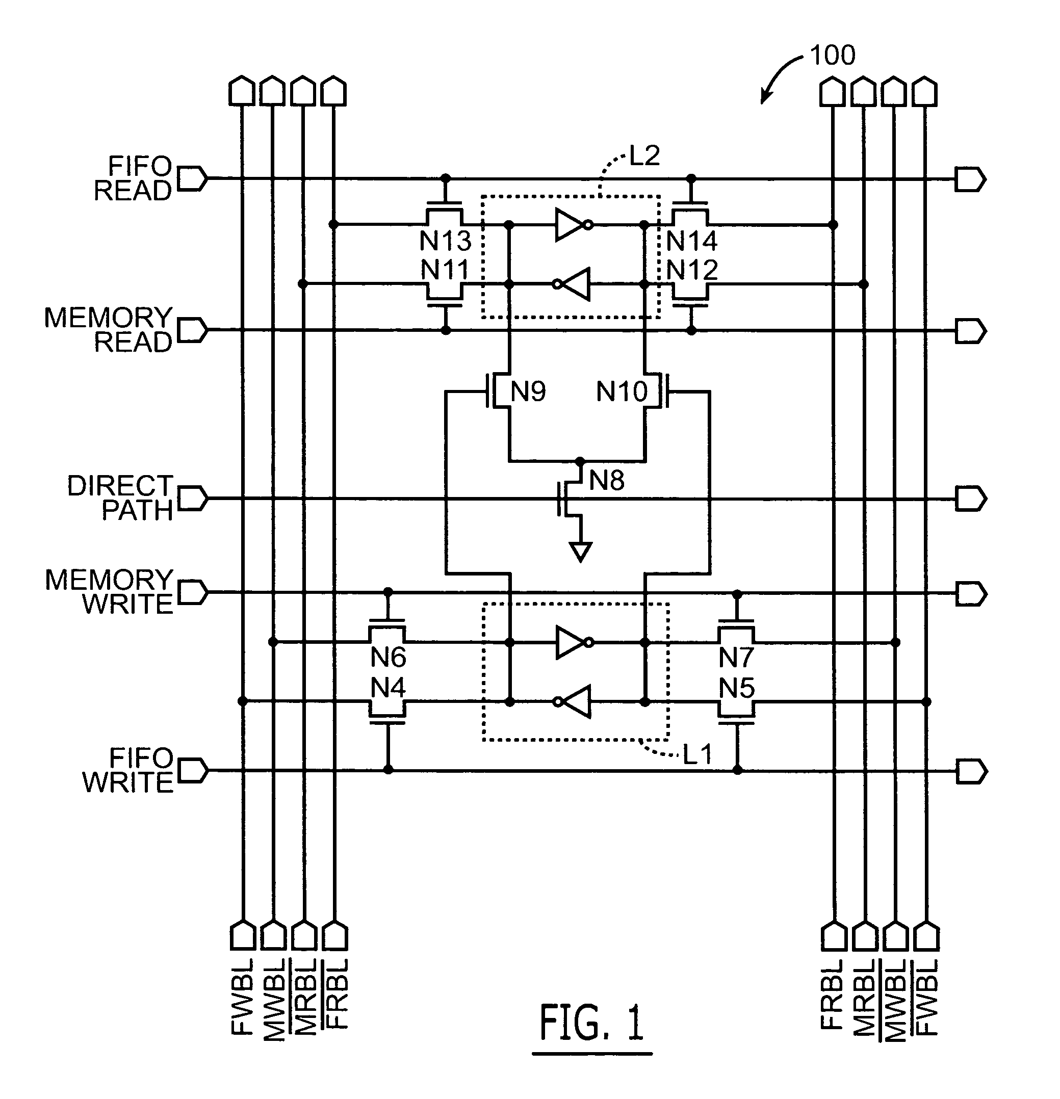
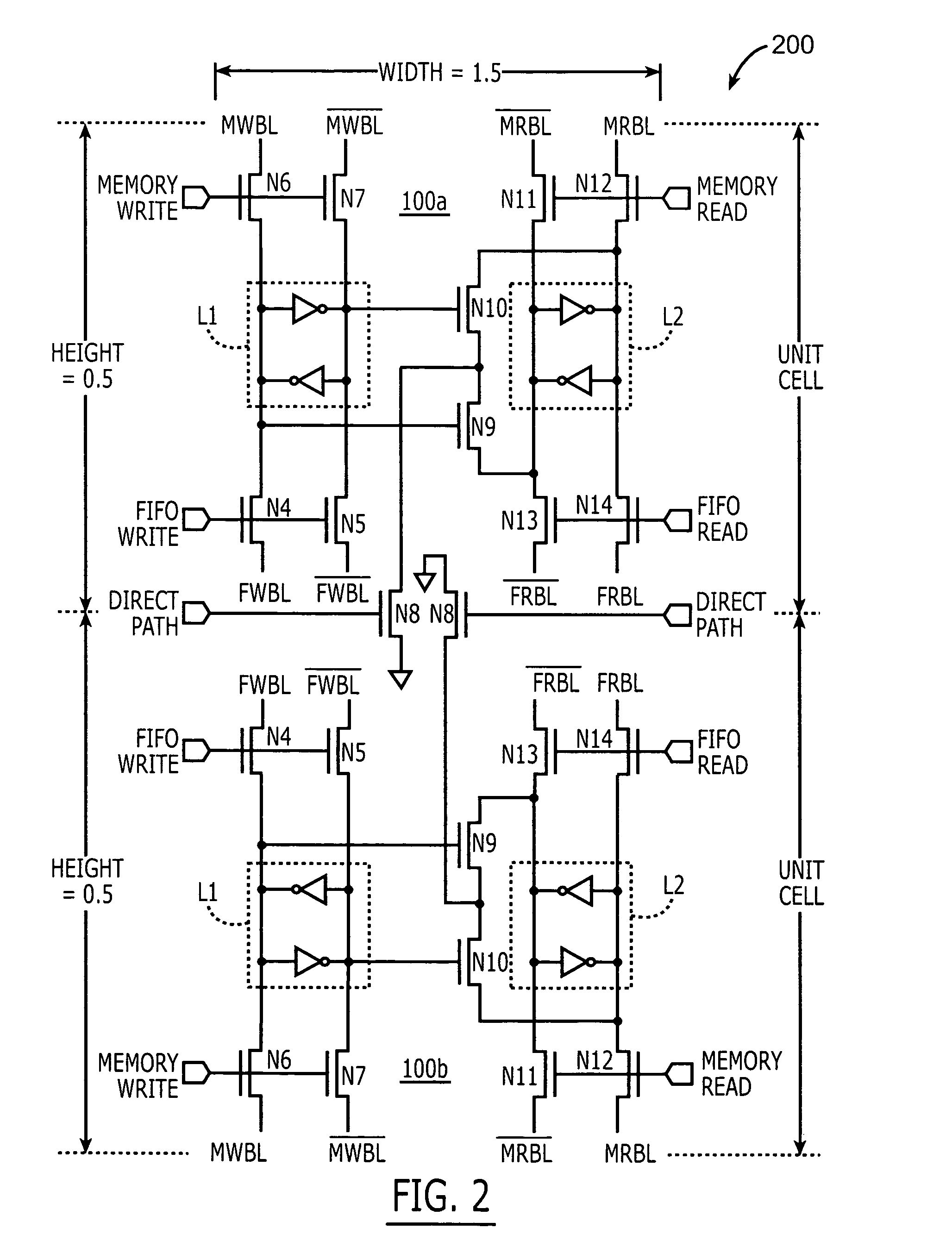
[0018]The present invention will now be described more fully herein with reference to the accompanying drawings, in which preferred embodiments of the invention are shown. This invention may, however, be embodied in many different forms and should not be construed as being limited to the embodiments set forth herein; rather, these embodiments are provided so that this disclosure will be thorough and complete, and will fully convey the scope of the invention to those skilled in the art. Like reference numerals refer to like elements throughout and signal lines and signals thereon may be referred to by the same reference characters. When added as a prefix, the symbol “ / ” designates a complementary data or information signal or an active low control signal, for example.

[0019]Embodiments of the present invention may be used as cache memory bit cells in such devices as first-in first-out (FIFO) memories and other sequential flow control devices. An exemplary sequential flow control devic...


PUM


Abstract

A multi-port memory cell includes a first SRAM element having a first pair of access transistors electrically coupled to a pair of FIFO write bit lines. A second dual-port SRAM element is also provided. This second dual-port SRAM element has a second pair of access transistors electrically coupled to a pair of FIFO read bit lines and a third pair of access transistors electrically coupled to a pair of memory read bit lines. A direct path data transfer circuit is provided. This transfer circuit is configured to support a unidirectional data transfer path that extends from first storage nodes within the first SRAM element to second storage nodes within the second dual-port SRAM element. This transfer circuit is also responsive to a direct path word line signal.

Description

CLAIM TO PRIORITY APPLICATION[0001]This application claims priority to U.S. Provisional Application Ser. No. 60 / 536,293, filed Jan. 14, 2004, the disclosure of which is hereby incorporated herein by reference.FIELD OF THE INVENTION[0002]The present invention relates to integrated circuit memory devices and methods of operating same, and more particularly to multi-port memory cells and memory cell layouts.BACKGROUND OF THE INVENTION[0003]Semiconductor memory devices can typically be classified on the basis of memory functionality, data access patterns and the nature of the data storage mechanism. For example, distinctions are typically made between read-only memory (ROM) devices and read-write memory (RWM) devices. The RWM devices typically have the advantage of offering both read and write functionality with comparable data access times. Typically, in RWM devices, data is stored either in flip-flops for “static” memory devices or as preset levels of charge on a capacitor in “dynamic...

Claims


Application Information

Patent Timeline
Patent Type & Authority Patents(United States)
IPC IPC(8): G11C8/00
CPCG11C8/16
Inventor LEE, SHIH-KEDAU, MARIO
Owner INTEGRATED DEVICE TECH INC
Why Eureka
Try Eureka