Methods and apparatus for verifying circuit board design

a circuit board and design technology, applied in the direction of testing circuits, instruments, program control, etc., can solve the problems of the degree of influence of each of the parts, the inability of the plate to connect to the other by an electric conductor, and the inability to find gaps by visual inspection in a miniaturized high-density mounting printed circuit board, etc., to achieve the effect of easy setting of priorities, easy decision of priorities, and easy priority setting

Inactive Publication Date: 2006-05-09
SONY CORP
View PDF20 Cites 3 Cited by
  • Summary
  • Abstract
  • Description
  • Claims
  • Application Information

AI Technical Summary

Benefits of technology

[0017]The invention is accomplished to provide a method and apparatus for verifying a circuit board design, which are enabled to reliably and easily make decisions an amount of electromagnetic wave radiation and on priorities respectively assigned to parts, to which countermeasures are applied, and to provide a method and apparatus for verifying a circuit board design, which are enabled to easily make decisions on parts, on which connectors are to be mounted, and to which countermeasures for suppressing electromagnetic wave radiation should be applied.
[0024]In accordance with the method for verifying a circuit board design according to the present invention, in a case where there are plural chippings in a power layer, a common-mode voltage is computed correspondingly to each of the chippings. A common-mode voltage value is indicated together with a position of the associated chipping. Thus, the priorities of the chippings, for which the countermeasure for suppressing radiation of electromagnetic waves is required, can easily be decided.
[0025]The apparatus for verifying a circuit board design according to the present invention is realized by adding a constituent element having the function of measuring a common-mode voltage to constituent elements, such as a detecting portion, a computing portion and an output portion, which a circuit-board design verifying apparatus usually have. Therefore, in the apparatus having a constituent element implemented by a microcomputer, the realization of such a function can be achieved by changing a control program. When seeing indications outputted from the output portion, an operator can easily decide the priorities of the chippings for which the countermeasure for suppressing radiation of electromagnetic waves is required.
[0026]In accordance with another method for verifying a circuit board design according to the present invention, priorities for applying a countermeasure to chippings can easily be set, similarly as the case of performing the aforementioned method for verifying a circuit board design. Moreover, the propagation value of a common-mode voltage reaching the connector, which serves as an antenna for electromagnetic wave radiation by being connected to a cable, can be obtained by computing. Thus, in a case where there are plural connectors, the priorities of the connectors or the cables, for which the countermeasure for suppressing radiation of electromagnetic waves is required, can easily be decided.
[0027]Another apparatus for verifying a circuit board design according to the present invention is realized by adding a constituent element having the functions of measuring a common-mode voltage and computing the propagation value thereof to constituent elements, such as a detecting portion, a computing portion and an output portion, which a circuit-board design verifying apparatus usually have. Therefore, in the apparatus having a constituent element implemented by a microcomputer, the realization of these functions can be achieved by changing a control program. When seeing indications outputted from the output portion, an operator can easily decide the priorities of the connectors or the cables, for which the countermeasure for suppressing radiation of electromagnetic waves is required, similarly as the case of performing the method for verifying a circuit board design, which has been described immediately above.

Problems solved by technology

However, even when this measure is used, it is frequent that the plates cannot be connected to each other by an electric conductor, for instance, in a case that different voltages are actually applied to between the power supply plates.
Although electromagnetic wave radiation is reduced when dimensions of the gap are small, it is not easily determined what dimensions of the gap are sufficient to reduce the electromagnetic wave radiation to an extent that resultant electromagnetic wave radiation is small enough to be ignored.
It takes much time and effort to find a gap by visual inspection in a miniaturized high-density mounting printed circuit board.
However, the technique described in the aforementioned official gazette has a drawback that in a case where many parts of the circuit board, which are referred to as the slots (see FIG. 12B) and the slits (see FIG. 12A), are to be adjusted, the degree of influence of each of the parts, which are to be adjusted, on occurrences of an electromagnetic wave radiation cannot be determined, and priorities for adjusting each of the parts, according to which one of the parts is determined so that the adjustment is started therefrom, cannot easily be known.
Thus, there is possibility that the parts each generating a large amount of electromagnetic wave radiation cannot be completely adjusted within a circuit board designing period when using a verifying method and a verifying system described in the aforementioned official gazette.
In this case, electromagnetic wave radiation from the entire printed circuit board cannot be effectively suppressed.
In a case where one of a plurality of power layers completely separated from each other in the same plane is set to be a target plate to be verified, the technique described in the aforementioned official gazette has another drawback in that wirings (signal lines) transversing above both the separated plates cannot be recognized by the verifying system as a part to be adjusted.
Consequently, the verifying method and system described in the aforementioned official gazette have a disadvantage that an amount of electromagnetic wave radiation generated from the entire printed circuit board cannot effectively be suppressed.
However, the method and system described in the aforementioned official gazette have still another drawback in that in a case of providing a plurality of connectors on the circuit board, the system cannot obtain information indicating which of the connectors should be selected as the one corresponding to a part to which countermeasures for suppressing electromagnetic wave radiation are applied, and that thus, a complete verification of the circuit board design cannot be performed.

Method used


Image

  • Methods and apparatus for verifying circuit board design
  • Methods and apparatus for verifying circuit board design
  • Methods and apparatus for verifying circuit board design

Examples


Embodiment Construction

[0041]Hereinafter, preferred embodiments of a method and an apparatus for verifying a circuit board design according to the invention will be described in detail with reference to the accompanying drawings.

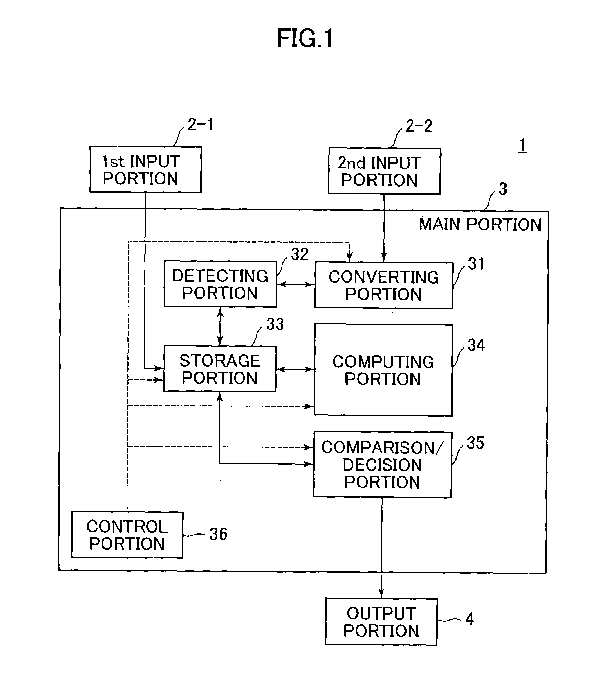
[0042]FIG. 1 is a schematic block view illustrating the configuration of a verifying apparatus for verifying a circuit board design according to an embodiment of the invention.

[0043]A verifying apparatus 1 shown in FIG. 1 has a first input portion 2-1 and a second input portion 2-2, which are used for inputting various data, and a main portion 3 centered on a computer, and also has an output portion 4.

[0044]The first input portion 2-1 is constituted by input equipment, such as a keyboard, or an input interface, and is used for inputting initial condition data online or offline. The second input portion 2-2 is an input interface for inputting board data and IBIS (I / O Buffer Information Specification) model data online or offline after a tentative design is created. Alternatively, t...


PUM


Abstract

The present invention provides a method for verifying a design of a circuit board that has a wiring layer connecting components to be mounted, a power layer, and an insulating layer formed between the wiring layer and the power layer. According to this method, detection of chippings in the power layer is performed. The chipping is, for example, a gap, a slot, or a slit, and corresponds to one wiring layer and interrupts a region in which the wiring layer and the power layer are opposed to each other. When chippings are detected, a common-mode voltage expected to be caused owing to each of the chippings is computed. Subsequently, the position of the chipping and the value of the common-mode voltage caused owing to the chipping are outputted. Thus, the priorities of the chippings, to which countermeasure for suppressing radiation of electromagnetic waves should be applied, can easily be decided.

Description

CROSS REFERENCES TO RELATED APPLICATIONS[0001]The present document is based on Japanese Priority Document JP 2002-190857, filed in the Japanese Patent Office on Jun. 28, 2002, the entire contents of which being incorporated herein by reference.BACKGROUND OF THE INVENTION[0002]1. Field of the Invention[0003]The present invention relates to a method and an apparatus for verifying influence of chippings, which are caused in a power supply layer, on electromagnetic wave radiation in a circuit board in which a wiring layer between components to be mounted faces the power supply layer through an insulating layer intervening between the wiring layer and the power supply layer.[0004]2. Description of Related Art[0005]A printed circuit board for use in recent electronic equipment is provided with conductive layers, to each of which a plurality of power supply voltages are applied, and conductive layers to be separated according to power supply voltages from each other and to be held at a com...

Claims


Application Information

Patent Timeline
Patent Type & Authority Patents(United States)
IPC IPC(8): G06F17/50G01R31/08G06F19/00G01R31/02H05K3/00
CPCG06F17/5036G06F30/367
Inventor ARAKI, KENJIYOKOYAMA, AYAO
Owner SONY CORP
Why Eureka
Try Eureka