Thin film encapsulation of MEMS devices

a technology of mems devices and thin films, applied in the field of microelectromechanical systems, can solve the problems of increasing the separation time, affecting the switching speed and response of the device, and the general sensitivity of the mems device to environmental conditions, so as to reduce the size and cost of the electronic system

Inactive Publication Date: 2006-05-16
NORTHROP GRUMMAN SYST CORP
View PDF17 Cites 45 Cited by
  • Summary
  • Abstract
  • Description
  • Claims
  • Application Information

AI Technical Summary

Benefits of technology

[0013]Some of the advantages of the MEMS devices according to the present invention are that they are sealed against particulate and vapor contamination while still in the controlled environment of a clean room, they can be sawed, handled and integrated into electronic systems using standard IC techniques without being contaminated or otherwise damaged, they do not need to be positioned on a top surface to be vertically integrated, and they can significantly reduce the size and cost of electronic systems employing MEMS devices by eliminating the need to hermetically seal the entire system.

Problems solved by technology

A disadvantage of MEMS devices in general is their sensitivity to environmental conditions.
Stiction is an adhesive or electrostatic attraction between electrodes that can have a negative impact on the switching speed and response of the device.
Any residual, unwanted attraction between electrodes will increase the time for separation, thereby decreasing switching speed.
In extreme cases, stiction may bind a MEMS switch in the closed position, thus rendering it inoperable.
A disadvantage of this approach is that it dramatically increases the size and cost of the system and, in addition, tends to limit the position of the MEMS device to an exposed surface of the system.
The increase in size also necessitates long vias to connect the MEMS device with radiators and other components leading to RF losses and increased noise, particularly at high frequencies (i.e., at or above 10 GHz).
A problem with this approach is that the mating process requires significant handling of the MEMS devices in an unprotected condition.
If a number of MEMS devices are formed in a batch on a single wafer, it is also necessary to saw the wafer with the MEMS devices in an unprotected condition thereby increasing the risk of damage to the devices.
It is also difficult to achieve and maintain a hermetic seal because of the variety of materials used.
A disadvantage of this approach is that it requires precise alignment of the wafers when bonding and complicates subsequent sawing operations.
This approach also leads to a significant increase in the overall size of each MEMS device because of the need to use a relatively thick wafer for creation of the cavities.

Method used


Image

  • Thin film encapsulation of MEMS devices
  • Thin film encapsulation of MEMS devices
  • Thin film encapsulation of MEMS devices

Examples


first embodiment

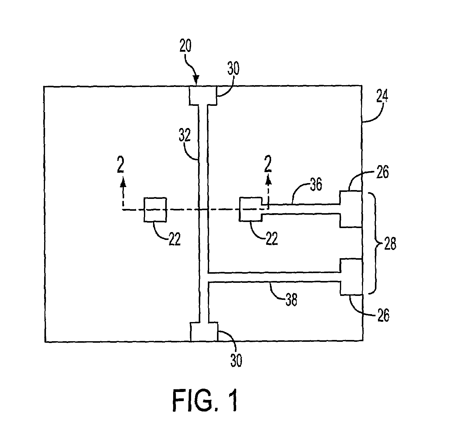
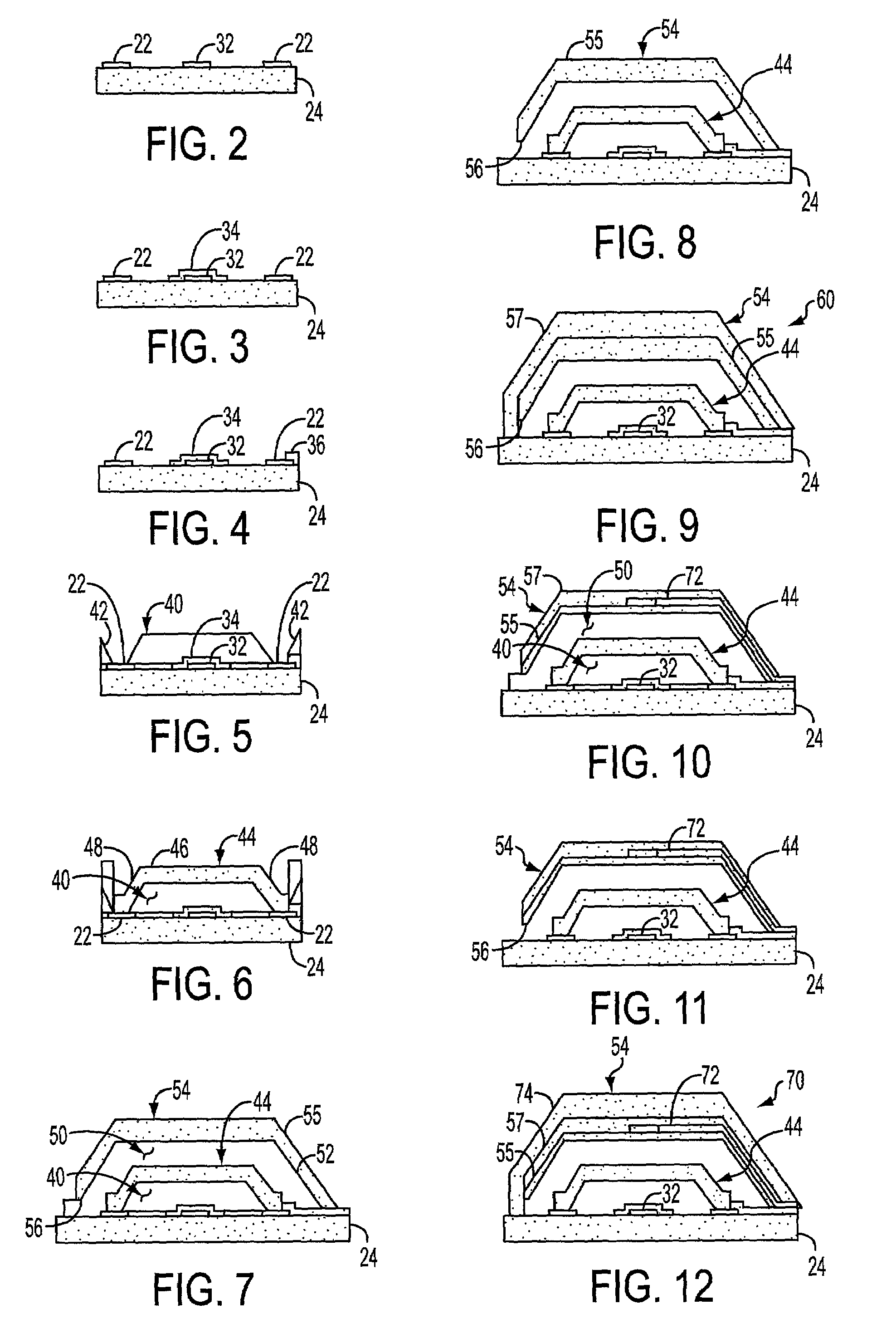
[0018]A method of manufacturing a MEMS device according to the present invention is illustrated in FIGS. 1–9. The method can be used to manufacture a variety of MEMS devices but is particularly advantageous when used to manufacture a two electrode switch for radio frequency (RF) applications as shown and described herein.

[0019]In the first step, illustrated in FIGS. 1 and 2, a first signal network 20 and anchor pads 22 for a movable member are formed on a substrate 24. Bond pads 26 for a control circuit 28 can also be formed on the substrate 24 in this step. The first signal network 20 shown in FIG. 1 includes a pair of bond pads 30 located at opposite edges of the substrate 24 and a stripline 32, which also acts as an actuating element, which is described in detail below extending between the bond pads 30 to function as a first electrode. The first signal network 20 and pads 22 can be formed on the substrate 24 in any conventional manner but are preferably formed using a lift-off p...

second embodiment

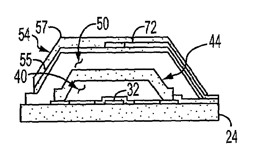
[0033]Another method of manufacturing a MEMS device according to the present invention involves performing the steps illustrated in FIGS. 10–12 after the steps illustrated in FIGS. 1–7. The resulting MEMS device 70 includes a counter electrode 72 embedded in the helmet 54 in addition to an electrode 32 on the substrate 24 such that the moving member 44 is disposed between a pair of electrodes.

[0034]The first through sixth steps of the second embodiment are performed in the same manner as described above to provide an intermediate product with a first encapsulant layer 55 disposed over and around the moving member 44 and the sacrificial layers 40 and 50.

[0035]In the seventh step of the second embodiment, illustrated in FIG. 10, a counter electrode 72 is defined on the first encapsulant layer 55, and an optional second encapsulant layer 57 is defined on the first encapsulant layer thereby covering the counter electrode. The counter electrode 72 can be formed of any electrically conduc...


PUM

PropertyMeasurementUnit
frequenciesaaaaaaaaaa
temperatureaaaaaaaaaa
thicknessaaaaaaaaaa

Abstract

A method of manufacturing a miniature electromechanical system (MEMS) device includes the steps of forming a moving member on a first substrate such that a first sacrificial layer is disposed between the moving member and the substrate, encapsulating the moving member, including the first sacrificial layer, with a second sacrificial layer, coating the encapsulating second sacrificial layer with a first film formed of a material that establishes an hermetic seal with the substrate, and removing the first and second sacrificial layers.

Description

BACKGROUND OF THE INVENTION[0001]1. Field of the Invention[0002]The present invention relates generally to micro-electromechanical systems (MEMS) and, in particular, to a method of encapsulating one or more MEMS devices formed on a substrate.[0003]2. Discussion of the Background Art[0004]Switching devices are used in electronic applications to connect and disconnect electrical signal paths. In radio frequency (RF) and microwave applications, it is desirable to form switches using micro-electromechanical system (MEMS) technology because such switches exhibit low insertion loss and high isolation capability compared to transistor switches especially at frequencies in the GHZ and above. A typical MEMS switch, such as described in U.S. Pat. No. 5,619,061 to Goldsmith et al., includes an electrode in the form of a horizontal beam element with at least one end clamped, hinged or anchored to a post, spacer, via or other type of stationary vertical structure. Another electrode is disposed i...

Claims


Application Information

Patent Timeline
Patent Type & Authority Patents(United States)
IPC IPC(8): H01L21/44B81C1/00B81B3/00B81B7/00B81B7/02
CPCB81C1/00293B81C2203/0136
Inventor FREIDHOFF, CARL B.
Owner NORTHROP GRUMMAN SYST CORP
Why Eureka
Try Eureka