

Display and driving method thereof
a technology of display and driving method, applied in the field of display, can solve the problems of element current measurement method of passive matrix display, difficulty in actually assembling a constant current source drive circuit, disadvantageous in terms of light emission efficiency, etc., and achieve the effect of uniform display, free of aperture ratio reduction, and without reducing the panel aperture ratio
- Summary
- Abstract
- Description
- Claims
- Application Information
AI Technical Summary
Benefits of technology
Problems solved by technology
Method used
Image

Examples
embodiment 1
[Embodiment 1]
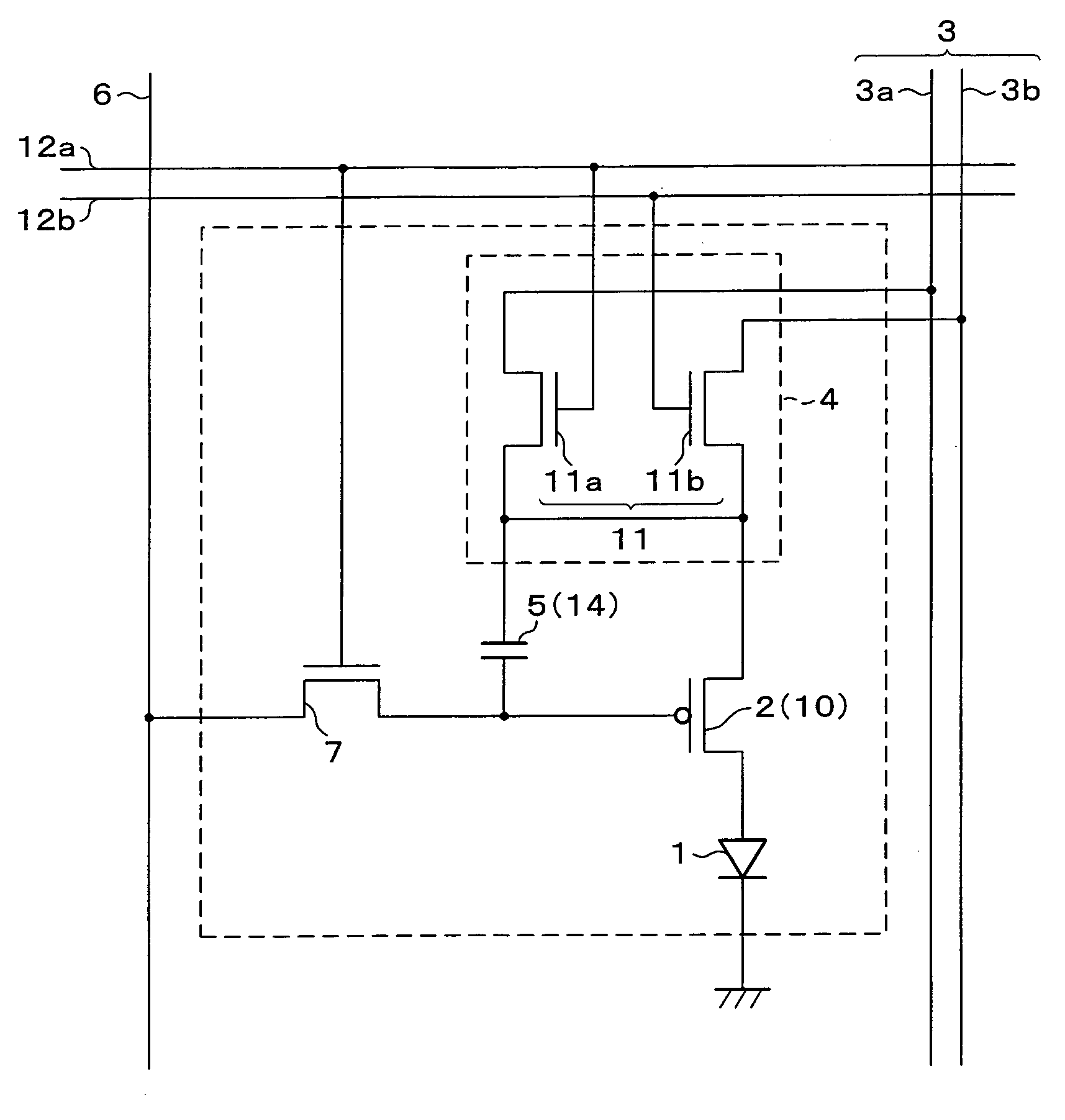
[0064]The following will describe an embodiment in accordance with the present invention. Although dealing with an organic EL display incorporating organic EL elements as light-emitting devices, the embodiment is by no means limiting the invention which is also applicable to any types of displays incorporating photoelectric elements adjusting luminance according to elements' current values, including the field emission display (FED).
[0065]The present embodiment will also describe an active matrix organic EL display as an organic EL display, because as already mentioned, with organic EL elements and other current-driven optical elements whose luminance is proportional to the current density therethrough, an active matrix structure in which each pixel has its own active element is advantageous over a passive (simple) matrix structure for better luminous efficiency and lower voltage.
[0066]In addition, in an active matrix structure, drivers and other TFT-based devices can ...
embodiment 2
[Embodiment 2]
[0111]The following will describe another embodiment in accordance with the present invention. Similarly to embodiment 1, the present embodiment will describe an active matrix organic EL display. Therefore, members of the present embodiment that have the same arrangement and function as members of embodiment 1, and that are mentioned in that embodiment are indicated by the same reference numerals and description thereof is omitted.
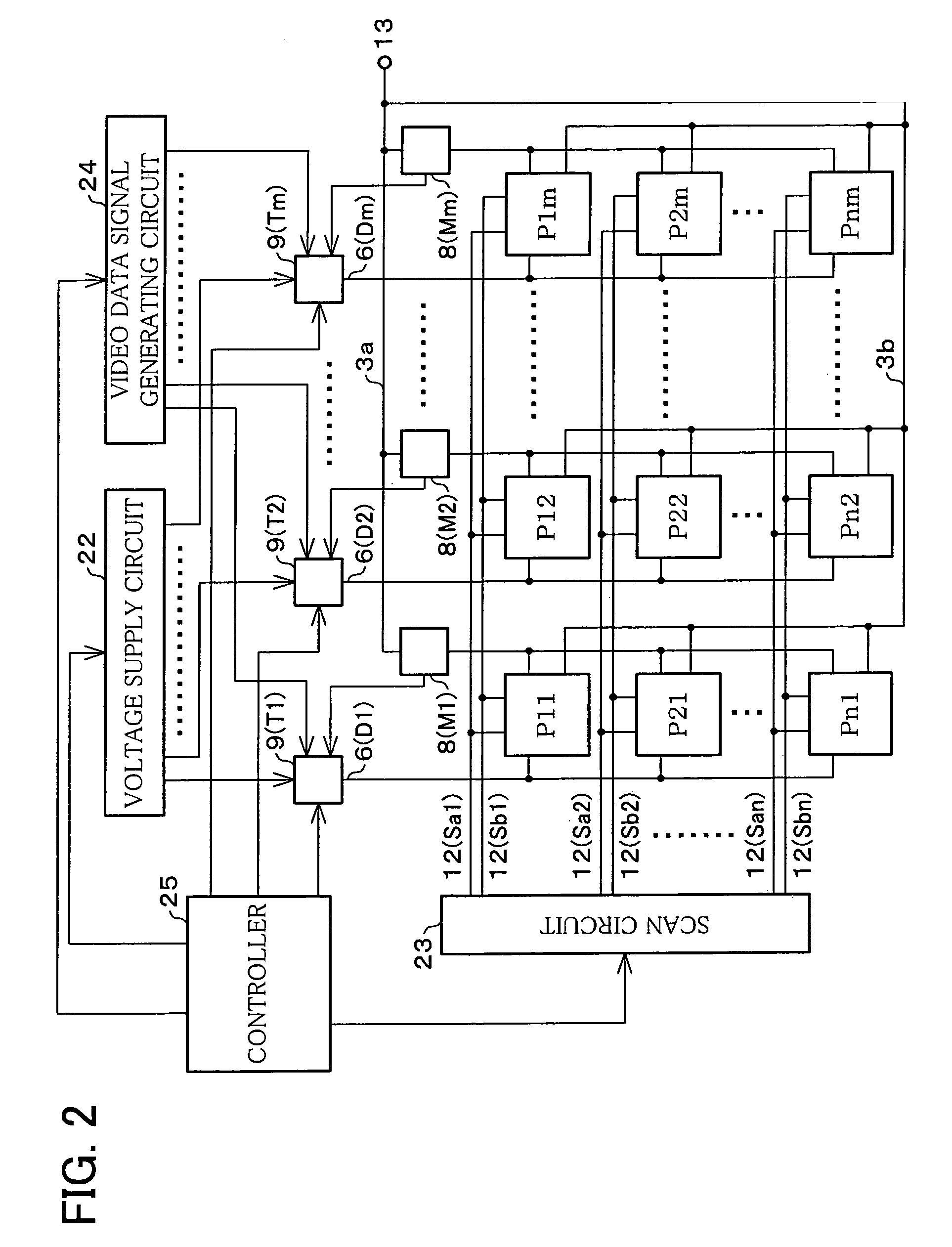
[0112]Referring to FIG. 7, the organic EL display of the present embodiment includes scan signal lines 12 and video data signal lines 6 which are positioned to form a matrix, and pixels P11 to Pnm, each complete with a photoelectric element 1 and an active element, which are located at the crossings of the two kinds of signal lines, similarly to those in the organic EL display of embodiment 1 (see FIG. 2).
[0113]In the organic EL display illustrated in FIG. 7, the scan signal line 12 associated with the pixels P11, P12, . . . , and P1m is deno...
PUM
 Abstract
Description
Claims
Application Information