Process control system and process control method

a control system and process control technology, applied in the field of process control system and process control method, can solve the problems of test wafers being left in an inspection wait state for a considerable time, test wafers may not always undergo all types of inspection, and the utilization schedule of these inspection devices is not well organized, so as to reduce the wafer processing cycle time, maximize the operating rate and production capacity in the area, and improve the operating rate of each processing apparatus

Active Publication Date: 2006-05-16
TOKYO ELECTRON LTD
View PDF8 Cites 20 Cited by
  • Summary
  • Abstract
  • Description
  • Claims
  • Application Information

AI Technical Summary

Benefits of technology

[0024]In order to achieve the object described above, a sixth aspect of the present invention provides a process control system installed for controlling processing executed on workpieces by at least one processing apparatus in each area in a factory and having a processing chamber in which the processing is executed on the workpieces, a measuring unit that executes measurement processing on a workpiece before and after the processing is executed on the workpiece in the processing chamber or either before or after the processing is executed on the workpiece in the processing chamber and a means for in-apparatus transfer capable of transferring the workpiece at least between the processing chamber and the measuring unit, which comprises at least one measuring apparatus installed in the corresponding area and capable of executing measurement processing on workpieces undergoing the processing within the area, a transfer apparatus installed in the area to transfer the workpieces among apparatuses within the area including the processing apparatus and the measuring apparatus and a control device installed in the area to control the processing apparatus, the measuring apparatus and the transfer apparatus in the area and implements control so as to engage the measuring unit of another processing apparatus to execute the measurement processing on a workpiece undergoing the processing executed by a given processing apparatus if the measuring unit of the given processing apparatus is not available for use. This system reduces the wafer processing cycle time in each area and, at the same time, maximizes the operating rate and the production capacity in the area.
[0025]According to the present invention, a process control system and a process control method that improve the operating rate of each processing apparatus while reducing the length of time (cycle time) to elapse from processing through inspection processing are provided.

Problems solved by technology

In addition, while there are various types of inspection devices, some test wafers may not always undergo all types of inspection.
However, the utilization schedules of these inspection devices are not well organized, resulting in some test wafers being left in an inspection wait state for a considerable length of time.
In addition, when test wafers are used to check the states of the processing apparatuses in correspondence to individual processing steps, the test wafers cannot be transferred to the processing apparatus which executes a different processing step until the inspection for the current processing step is completed.
Thus, it takes a considerable length of time to process the test wafers, leading to lower operating rates of the processing apparatuses.
In this case, a greater area in the clean room needs to be allocated for the installation of the two separate transfer paths, one for the production wafers and the other for the test wafers, and the wafers cannot be transferred quickly.

Method used


Image

  • Process control system and process control method
  • Process control system and process control method
  • Process control system and process control method

Examples


first embodiment

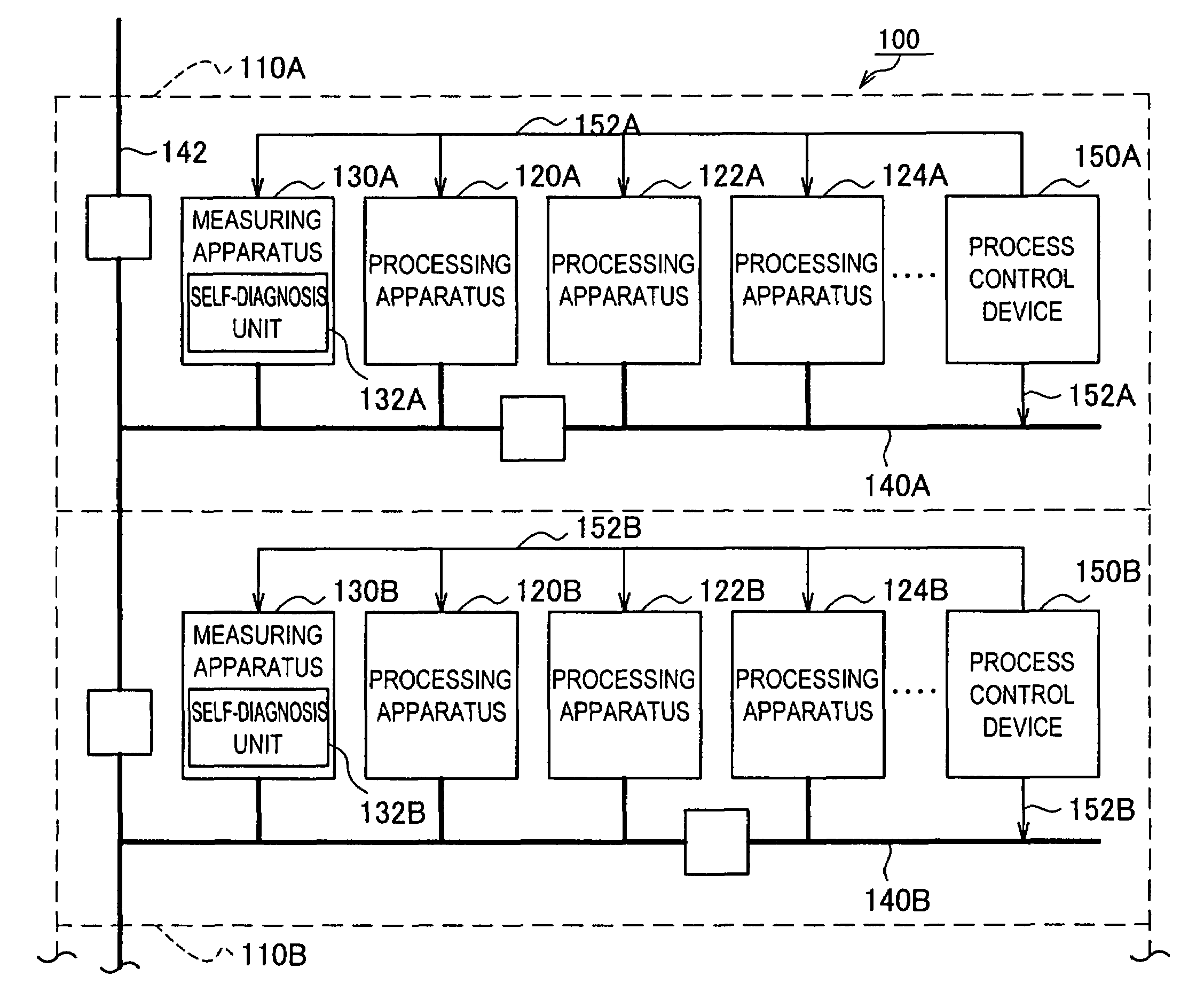
[0038]The process control system achieved in the first embodiment controls semiconductor device manufacturing processes. FIG. 1 schematically illustrates the overall structure of the process control system. The process control system 100 is installed in a clean room at, for instance, a semiconductor manufacturing plant.

[0039]The space inside the clean room is divided into a plurality of areas (to be referred to as “bays” in this document) 110 (110A, 110B . . . ). The number of bays in the clean room corresponds to the manufacturing steps that need to be executed to manufacture semiconductor devices.

[0040]In each bay 110 (110A, 110B . . . ), a plurality of processing apparatuses 120 (120A, 120B . . . ), 122 (122A, 122B . . . ), 124 (124A, 124B . . . ) that process wafers are installed. The processing apparatuses 120, 122, 124 . . . may be, for instance, etching apparatuses, CVD (chemical vapor deposition) apparatuses, coaters / developers, wafer cleaning tools, CMP (chemical mechanical...

second embodiment

[0103]Next, the present invention is explained in reference to the drawings. In this embodiment, the process control device 150 generates a model expression for predicting the results of the processing executed by the processing apparatuses 120, 122, 124 . . . . through a multivariate analysis and implements the process control based upon the model expression.

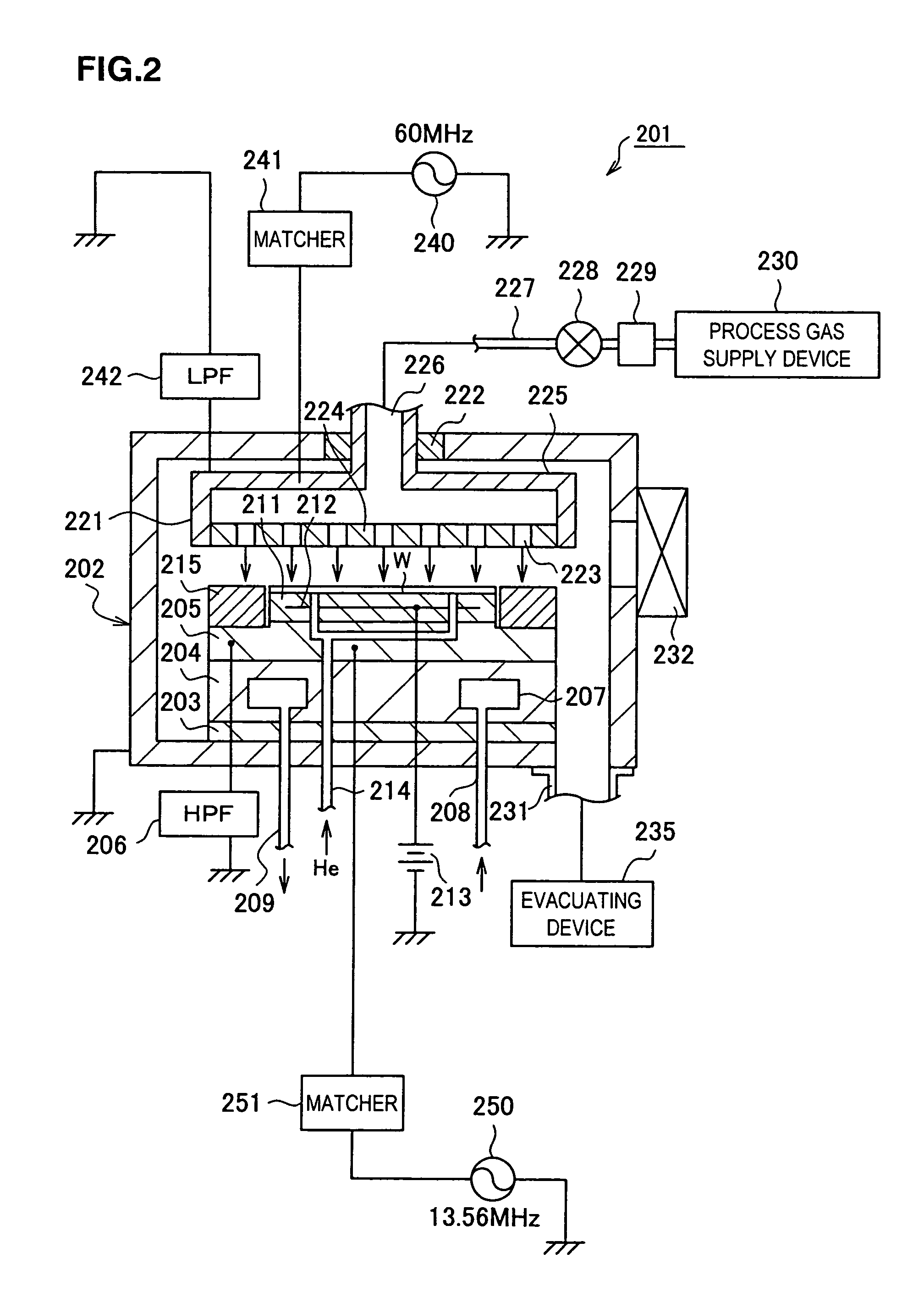
[0104]The processing apparatuses 120 in the embodiment are each identical to the etching apparatus 201 shown in FIG. 2. In addition, the process control device 150 includes a means for multivariate analysis 400 in the embodiment.

[0105]As shown in FIG. 6, the means for multivariate analysis 400 includes an operation data storage unit 410, a processing result data storage unit 420, a multivariate analysis program storage unit 430, a multivariate analysis processing unit 440 and a multivariate analysis result storage unit 450.

[0106]The operation data storage unit 410 constitutes a means for storing it in memory operation data, whe...


PUM


Abstract

A process control system that controls processing executed on semiconductor wafers by processing apparatuses 120, 122, 124 installed in each bay (area) 110 inside a factory the processing results of which are predictable, having installed in the corresponding bay, at least one measuring apparatus 130 that executes a measuring operation on workpieces undergoing the processing in the bay, a transfer path 140 of a transfer apparatus, through which the workpieces are transferred among various apparatuses installed within the bay including the individual processing apparatuses and the measuring apparatus and a process control device 150 that controls the processing apparatuses, the measuring apparatus and the transfer apparatus in the bay. This structure reduces the length of time (cycle time) to elapse from the processing through the inspection operation and also improves the operating rate of each processing apparatus.

Description

BACKGROUND OF THE INVENTION[0001]The present invention relates to a process control system and a process control method that may be adopted to implement control on processes through which semiconductor devices, for instance, are manufactured.[0002]In a semiconductor manufacturing factory, for instance, a plurality of process units are installed for semiconductor production. Each process unit includes a transfer apparatus that transfers workpieces such as semiconductor wafers (hereafter to be referred to simply as “wafers”) to a plurality of processing apparatuses such as etching apparatuses. In such a process unit, wafer processing is executed in a specific sequence while transferring the wafers to the individual processing apparatuses. Test wafers are normally used to regularly check the quality of process result in the etching apparatuses or the like. These test wafers undergo the processing mentioned above and then the etching rate, across wafer uniformity and the like of the tes...

Claims


Application Information

Patent Timeline
Patent Type & Authority Patents(United States)
IPC IPC(8): G06F19/00G05B19/418
CPCG05B19/41875G05B2219/33327G05B2219/45031G05B2219/37576G05B2219/37575Y02P90/02
Inventor TOMOYASU, MASAYUKI
Owner TOKYO ELECTRON LTD
Why Eureka
Try Eureka