Conductor-pattern testing method, and electro-optical device

a conductor pattern and test method technology, applied in the direction of static indicating devices, identification means, instruments, etc., can solve the problems of dust and acids, galvanic corrosion danger, etc., and achieve the effect of preventing the error detection resulting from the dummy pattern

Inactive Publication Date: 2006-05-23
BOE TECH GRP CO LTD
View PDF3 Cites 6 Cited by
  • Summary
  • Abstract
  • Description
  • Claims
  • Application Information

AI Technical Summary

Benefits of technology

[0016]According to the present invention, dummy conductors disposed in the array direction of the plurality of conductors are formed in segments, and two or more among the probes are prevented from being simultaneously in contact with the same dummy conductor. Thus, short-circuiting between probes, caused by the dummy conductors, does not occurs even when the at least two probes are progressively moved for inspection in the array direction of the plurality of conductors. This can prevent false determination, and can detect rapid and easy detection of a defect in the conductor pattern from the determination result.
[0018]The present invention serves to readily detect defects including short-circuiting between the electrodes or wiring lines formed on the base.
[0020]According to the present invention, by forming the dummy conductors so as to be set apart between any pair of probes in the extending direction of the conductors, short circuits between the probes are readily prevented while not making the dummy pattern too complex. When the dummy conductors are separated in the extending direction particularly be spacing lines (pattern gaps) extending in the array direction of the conductors, providing spacing lines in the number corresponding to the number of probe intervals will suffice to prevent short circuiting between the probes. It is to be noted that, in this application, being separated in the direction X indicates being separated so that there shall be no electrical conductivity in the direction X.
[0022]According to the present invention, by forming the dummy conductors so as to be shorter when viewed along the extending direction of the conductors than the minimum length between any pair of the probes in the extending direction of the conductors, short circuits between the probes do not occur even if the testing positions of a plurality of the probes are deviated in the extending direction of the conductors, and thus erroneous detection resulting from the dummy pattern may be prevented more adequately.
[0024]According to the present invention, by separating the dummy conductors in the array direction of the conductors in a pitch equivalent to the array pitch of the conductors, each of the probes, intended to contact respectively on distinct one of conductors, will contact respectively on distinct one of dummy conductors, preventing short circuits between the probes. It is further preferable to form the conductors and the dummy conductors so as to be in phase with each other. This ensures that each of the probes will respectively contact on distinct one of dummy conductors without altering the operation cycle of the probes, thereby further ensuring prevention of short circuits between the probes.
[0026]An electro-optical device according to the present invention includes: a conductor pattern constituted by a plurality of elongated conductors formed in parallel to each other on a base; a dummy pattern, which are not required to work as the conductors, constituted by a plurality of dummy conductors formed in an area on the base where the conductor pattern is not formed; and electro-optical material disposed on the conductor pattern. In the electro-optical device, the dummy conductors disposed in the array direction of the conductors to constitute the dummy pattern are mutually separated in the extending direction of the conductors. Each of the dummy conductors is preferably shorter when viewed along the extending direction of the conductors than the minimum length between any pair of the probes in the extending direction of the conductors. Thus, erroneous detection resulting from the dummy pattern may be prevented by forming each of the dummy conductors to be shorter than a certain length when viewed along the extending direction of the conductors and performing inspections with a probe interval not less than the particular length.

Problems solved by technology

The wiring lines 11b and 11c on the extended area 11s are formed with a small line width and in a fine pitch, and hence are vulnerable to dust and acids and also involves the danger of galvanic corrosion.

Method used


Image

  • Conductor-pattern testing method, and electro-optical device
  • Conductor-pattern testing method, and electro-optical device
  • Conductor-pattern testing method, and electro-optical device

Examples


Embodiment Construction

[0037]A method of inspecting a conductor pattern as well as an electro-optical device according to the present invention will now be described in detail in their preferred embodiments. It is to be noted that, although the embodiments described below are concerned with a method of inspecting an electrode pattern or a wiring pattern formed on a substrate (panel substrate) constituting a liquid crystal device (liquid crystal panel) as well as a construction of such a liquid crystal device, the present invention is applicable to a variety of conductor patterns not only to an electrode pattern or a wiring pattern on a substrate constituting a liquid crystal device, but also to a variety of electro-optical devices including luminescence devices or plasma display devices as well as liquid crystal devices.

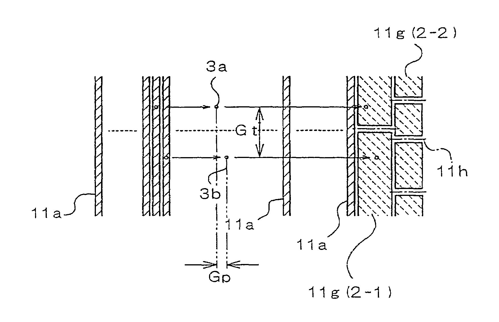
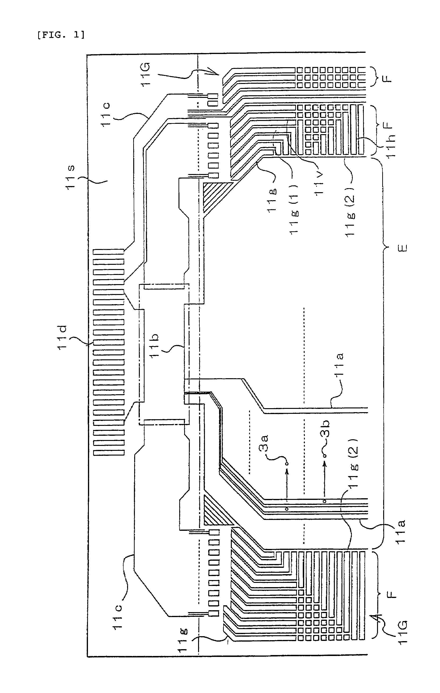
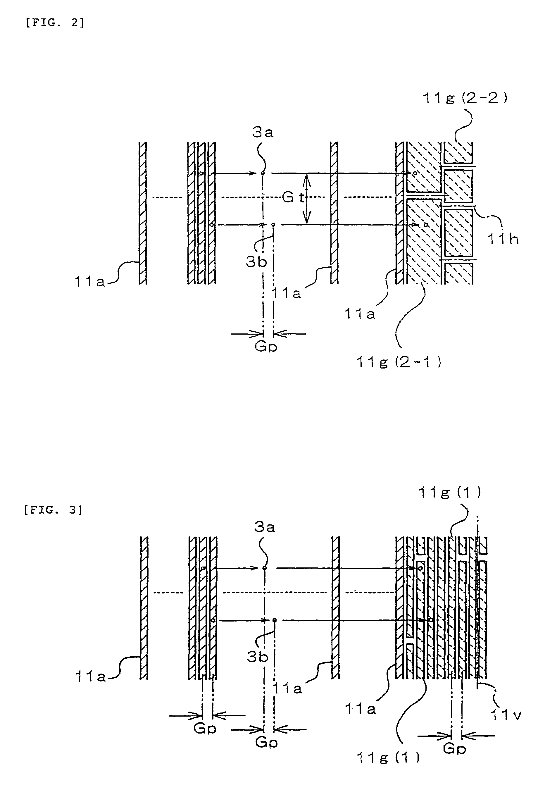
[0038]FIG. 1 is a fragmentary expanded plan view showing a part of a transparent substrate 11 constituting a liquid crystal device according to a preferred embodiment. The liquid crystal d...


PUM


Abstract

A conductor pattern having both elongated conductors and a dummy pattern is formed on a substrate. The dummy pattern is formed of dummy conductors. The elongated conductors are typically transparent electrodes. The dummy pattern is so configured that each of the dummy conductors are mutually set apart with a spacing as appropriate in the extending direction (top-and-bottom direction) and in the array direction (right-and-left direction) of the transparent electrodes to prevent any two inspection probes from contacting a single dummy conductor.

Description

BACKGROUND[0001]1. Technical Field of the Invention[0002]The present invention relates to a method of inspecting a conductor pattern as well as to electro-optical devices, and more specifically to a pattern structure which can be suitably implemented as an electrode pattern or a wiring pattern formed on a substrate constituting a liquid crystal panel and to a method of inspecting such a pattern.[0003]2. Description of the Related Art[0004]A typical liquid crystal device is formed by a pair of transparent substrates attached together via a sealant, with liquid crystals filled in the space between the two substrates and surrounded by the sealant, i.e., a liquid crystal sealed area.[0005]An example of liquid crystal device construction is shown in FIG. 4 and FIG. 5. FIG. 4 is a perspective plan view which schematically illustrates the planar structure of a liquid crystal device 10, while FIG. 5 is an expanded sectional view schematically showing the structure of the liquid crystal devi...

Claims


Application Information

Patent Timeline
IPC IPC(8): H01R12/04H05K1/11H05K3/00G01R31/02G01R31/28G02F1/13G02F1/1333G02F1/1345G09F9/00
CPCG02F1/1309G01R31/2818G09G3/006G02F2001/13456G02F2001/133388G02F1/133388G02F1/13456
Inventor MIYASAKA, KOICHI
Owner BOE TECH GRP CO LTD
Why Eureka
Try Eureka