Low power source driver for liquid crystal display

a technology of liquid crystal display and low power source, which is applied in the direction of instruments, static indicating devices, etc., can solve the problems of increasing the size of the integrated circuit device, increasing the manufacturing cost, and increasing the number of operational amplifiers with a large number of elements

Inactive Publication Date: 2006-05-23
HIMAX TECH LTD
View PDF4 Cites 10 Cited by
  • Summary
  • Abstract
  • Description
  • Claims
  • Application Information

AI Technical Summary

Benefits of technology

[0015]The LCD driving apparatus of the present invention constructed without the operational

Problems solved by technology

In the prior art driver, however, the number of operational amplifiers with a large number of elements increases with the number of data lines.
Therefore, if an LCD driving apparatus using the prior art driver is constructed in the form of a single integrated circuit device, the size of the integrated circuit device must be increased to accommodate enough operational amplifiers

Method used


Image

  • Low power source driver for liquid crystal display
  • Low power source driver for liquid crystal display
  • Low power source driver for liquid crystal display

Examples


first embodiment

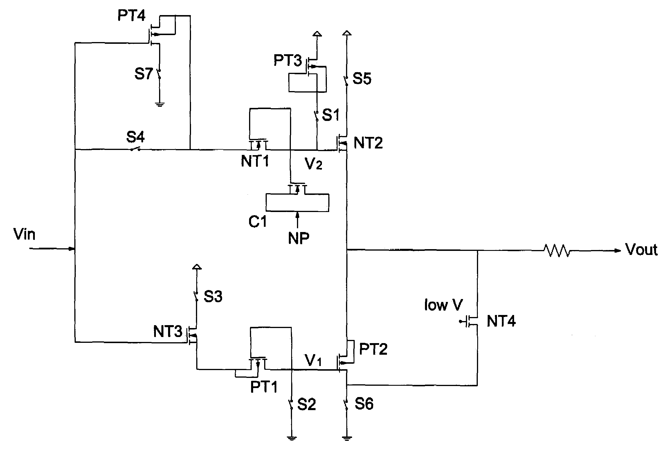
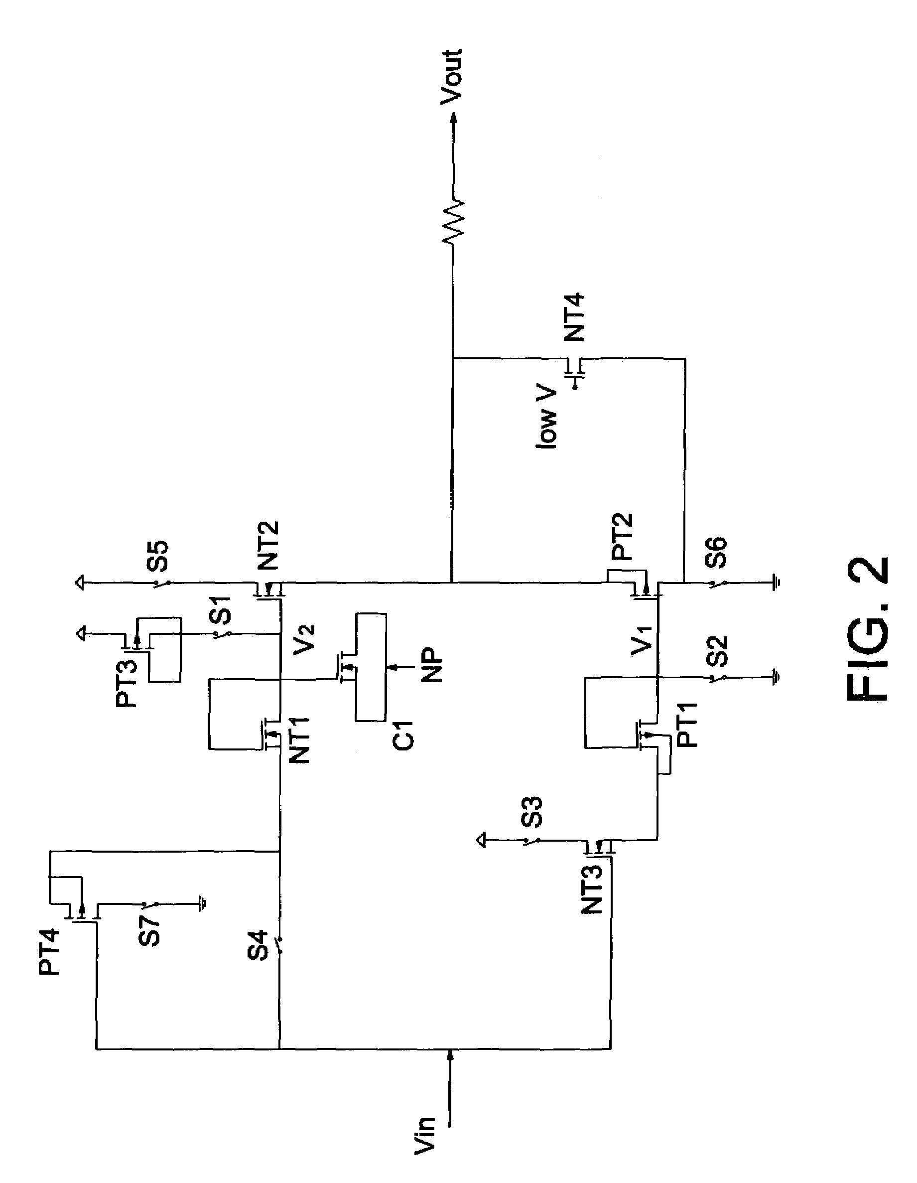
[0029]FIG. 2 shows a source driver according to the present invention. In the source driver of the present invention, first and second P-channel MOS transistors are used to trace the input voltage thereby eliminating the body effect in n-well process and keeping the loading charge loss constant. The first and second P-channel MOS transistors PT1, PT2 have a common gate connected to a drain of the first P-channel MOS transistor PT1, and the second P-channel MOS transistor PT2 has a source connected to an output terminal. First and second N-channel MOS transistors NT1, NT2 have a common gate connected to a drain of the first N-channel MOS transistor NT1, and the second N-channel MOS transistor NT2 has a source connected to the output terminal. A third N-channel MOS transistor NT3 has a gate connected to an input terminal, and a source connected to the source of the first P-channel MOS transistor PT1. A third P-channel MOS transistor PT3 has a drain connected to the power supply termin...

second embodiment

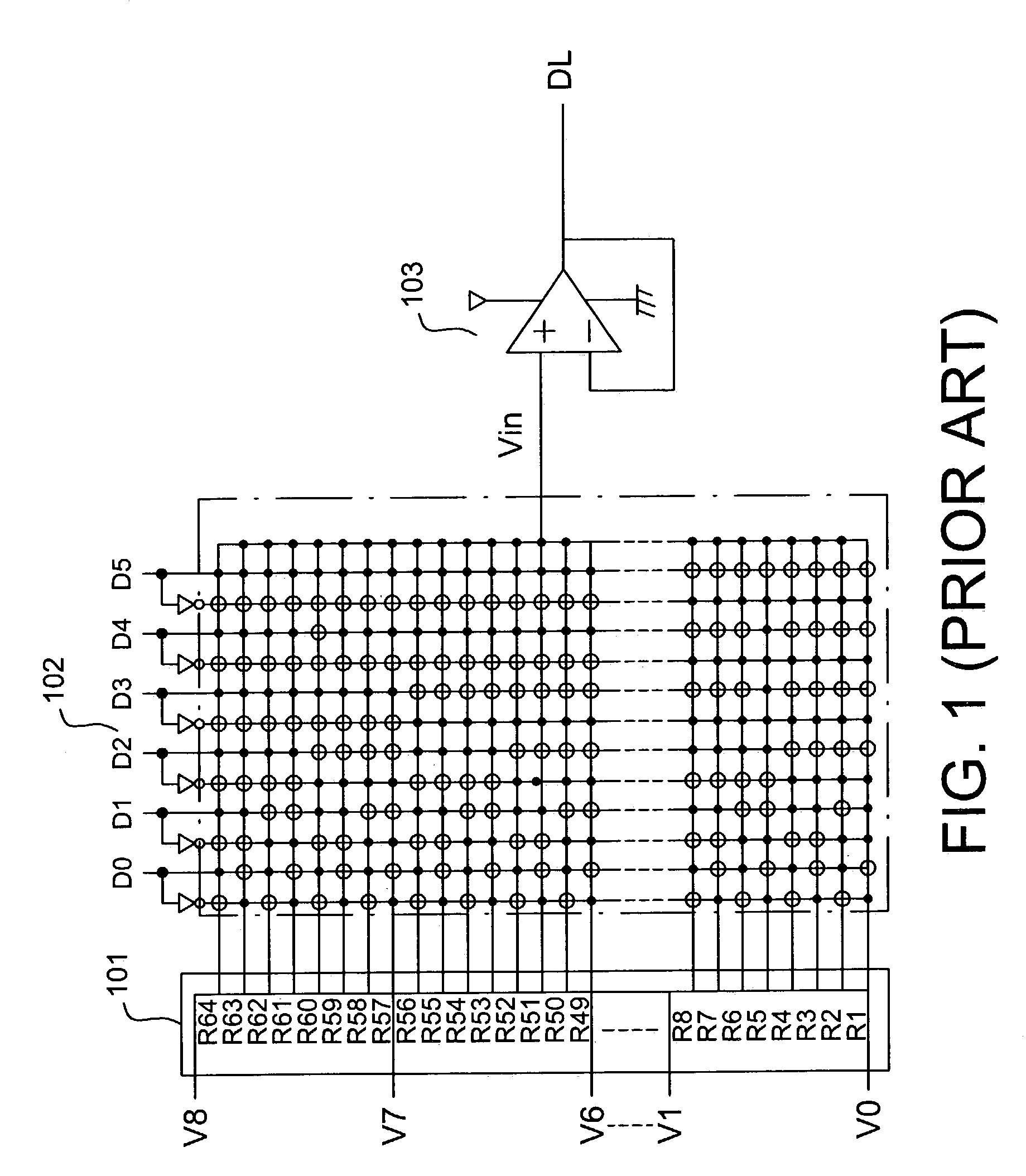
[0049]Since the source follower of P-channel MOS transistor cannot trace the low Gamma voltage, there still needs the source follower of N-channel MOS transistor to trace the low Gamma voltage. For example, the V0 expresses the highest Gamma voltage, the V63 expresses the lowest Gamma voltage. The Gamma voltages of V1, V2, . . . V62 are decreased in sequence. the driver according to the present invention separates the Gamma voltage into three parts. The Gamma voltages of part I are between V0 and V7. The Gamma voltages of part II are between V8 and V55. The Gamma voltages of part III are between V56 and V63.

[0050]FIGS. 7A through 7F show timing diagrams for explaining first operation of the driver of FIG. 6 in part I, which show a two-data output period. The switch S4 is always turned OFF in the part I and part II.

[0051]First, at time t0, as shown in FIG. 7B, the switches S1 and S2 are both turned ON. A bias voltage V1 at the gates of the transistors PT1 and PT2 is 0 volt. Also, a b...


PUM


Abstract

Disclosed is a source driver for receiving an input voltage and generating an output voltage to drive a data line in a liquid crystal display apparatus. In the source driver, first and second P-channel MOS transistors are together used as a primary source follower to trace the input voltage thereby eliminating the body effect and keeping the loading charge loss constant. First and second N-channel MOS transistors are used, as a secondary source follower. A capacitor is used for boosting the voltage of the drain of the first N-channel MOS transistor on the level of at least the input voltage plus the threshold voltage of the N-channel MOS transistor. In addition, an extra switch is used to reach the accurate output voltage when the output voltage is approaching the input voltage.

Description

BACKGROUND OF THE INVENTION[0001]1. Field of the Invention[0002]The present invention relates to an apparatus for driving a liquid crystal display (LCD) apparatus, and more particularly, to a low power source driver for use in the LCD driving apparatus.[0003]2. Description of the Related Art[0004]Since LCD panels are thinner in size and lower in power dissipation as compared with cathode-ray tube (CRT) panels, the LCD panels have recently been applied to personal computers, word processors, color telereceivers. Particularly, since active matrix-type LCD apparatuses have a high-speed response, a fine screen with a high quality, and a multi-gradation display, the active matrix-type LCD apparatuses have been in demand.[0005]Generally, an active matrix-type LCD apparatus is constructed by a semiconductor substrate having thin film metal wire, a transparent pixel electrodes and thin-film transistors (TFTs), a counter substrate having a transparent common electrode, and liquid crystal ins...

Claims


Application Information

Patent Timeline
IPC IPC(8): G09G3/36
CPCG09G3/3688G09G2330/021G09G2310/027G09G2300/0408
Inventor CHIU, MING CHENG
Owner HIMAX TECH LTD
Why Eureka
Try Eureka