Semiconductor integrated circuit device

a technology of integrated circuits and semiconductors, applied in solid-state devices, transmission, electromagnetic wave demodulation, etc., can solve the problems of deteriorating receiving sensitivity, affecting the self-heating influence of transistors around them, etc., to reduce thermal interference, improve the receiving sensitivity to signals, and prevent dc offset

Inactive Publication Date: 2006-05-23
HITACHI LTD +1
View PDF4 Cites 22 Cited by
  • Summary
  • Abstract
  • Description
  • Claims
  • Application Information

AI Technical Summary

Benefits of technology

[0010]Additionally, in order to prevent the DC offset due to the self heating of the transistors, the mixer section is in advance operated before reaching a receiving period, and can be also switched to the receiving mode at the time when the thermal interference between the transistors reaches its saturation. However, there are problems such that its useless current consumption is increased in this case and the awaiting time of the cellular phone etc. is shortened.
[0011]An object of the present invention is to provide a semiconductor integrated circuit device capable of largely improving the receiving sensitivity to the signals by reducing the thermal interference due to the self heating of each transistor constituting the gilbert cell circuit.

Problems solved by technology

However, the influence on the transistors around them due to the self heating is not equivalent depending on the layout of the transistors.
Therefore, a problem arises such that the DC offset occurs, which results in the deterioration of the receiving sensitivity, and the like.

Method used


Image

  • Semiconductor integrated circuit device
  • Semiconductor integrated circuit device
  • Semiconductor integrated circuit device

Examples


Embodiment Construction

[0030]Hereinafter, embodiments of the present invention will be described in detail based on the drawings.

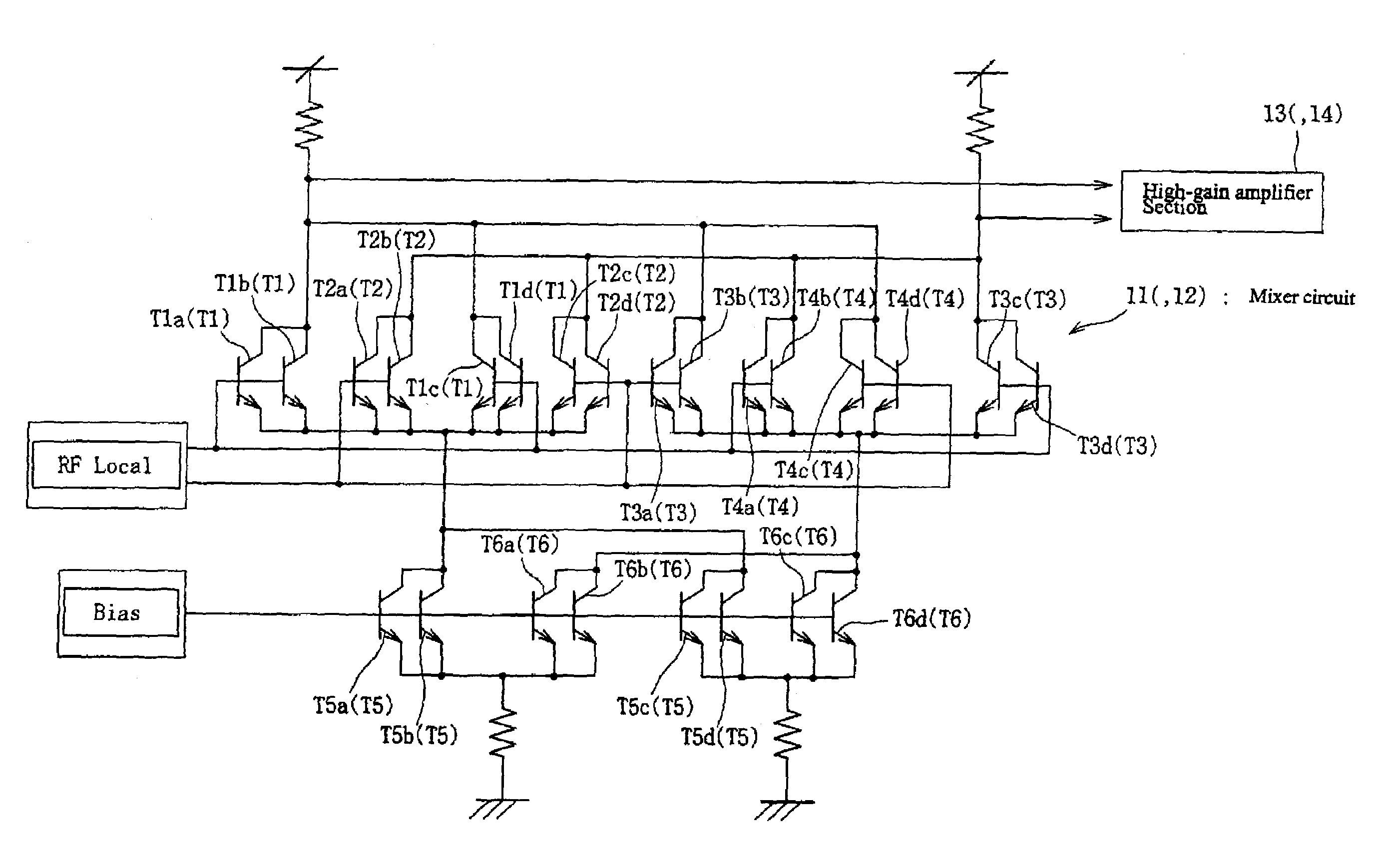
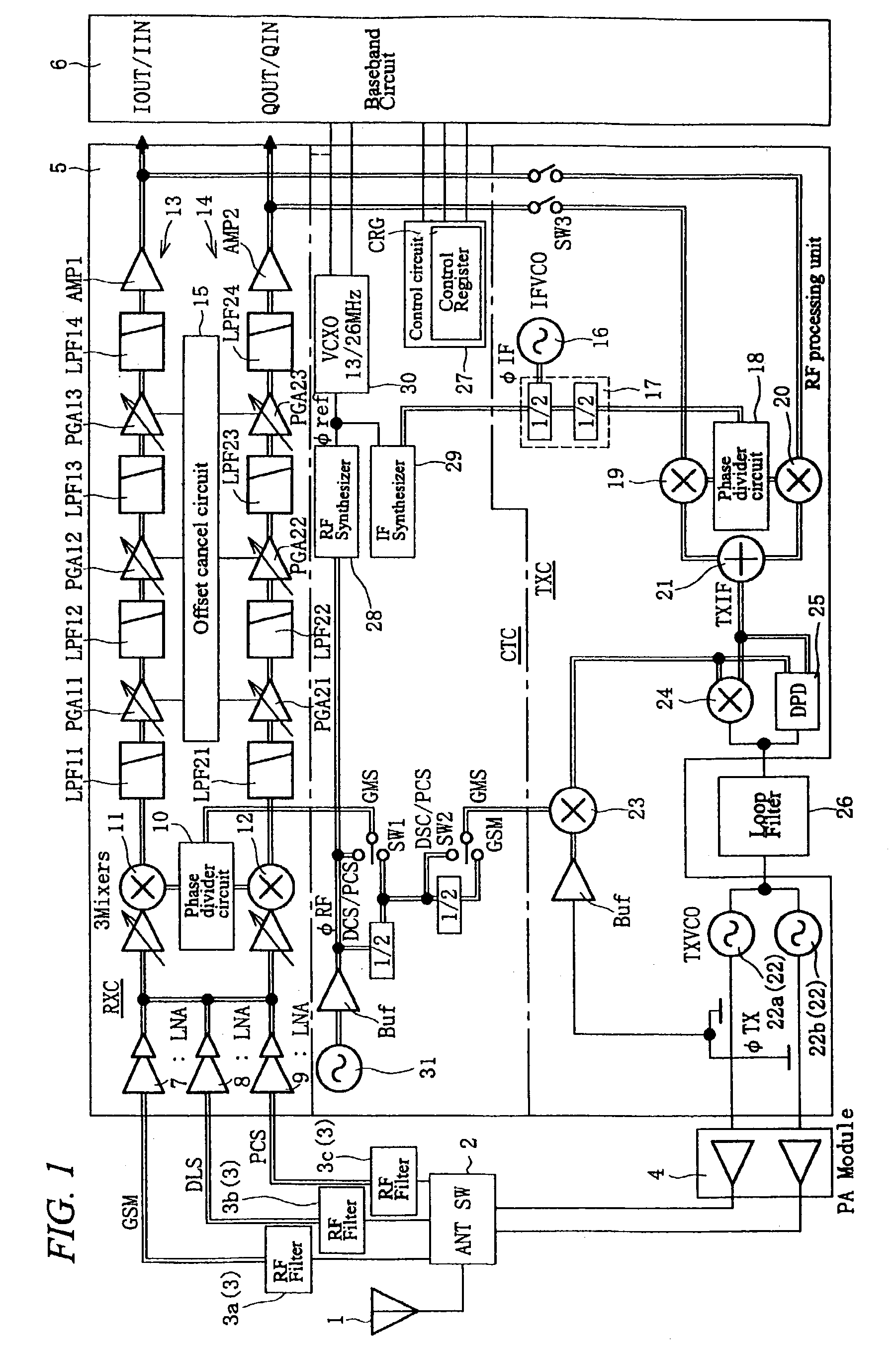
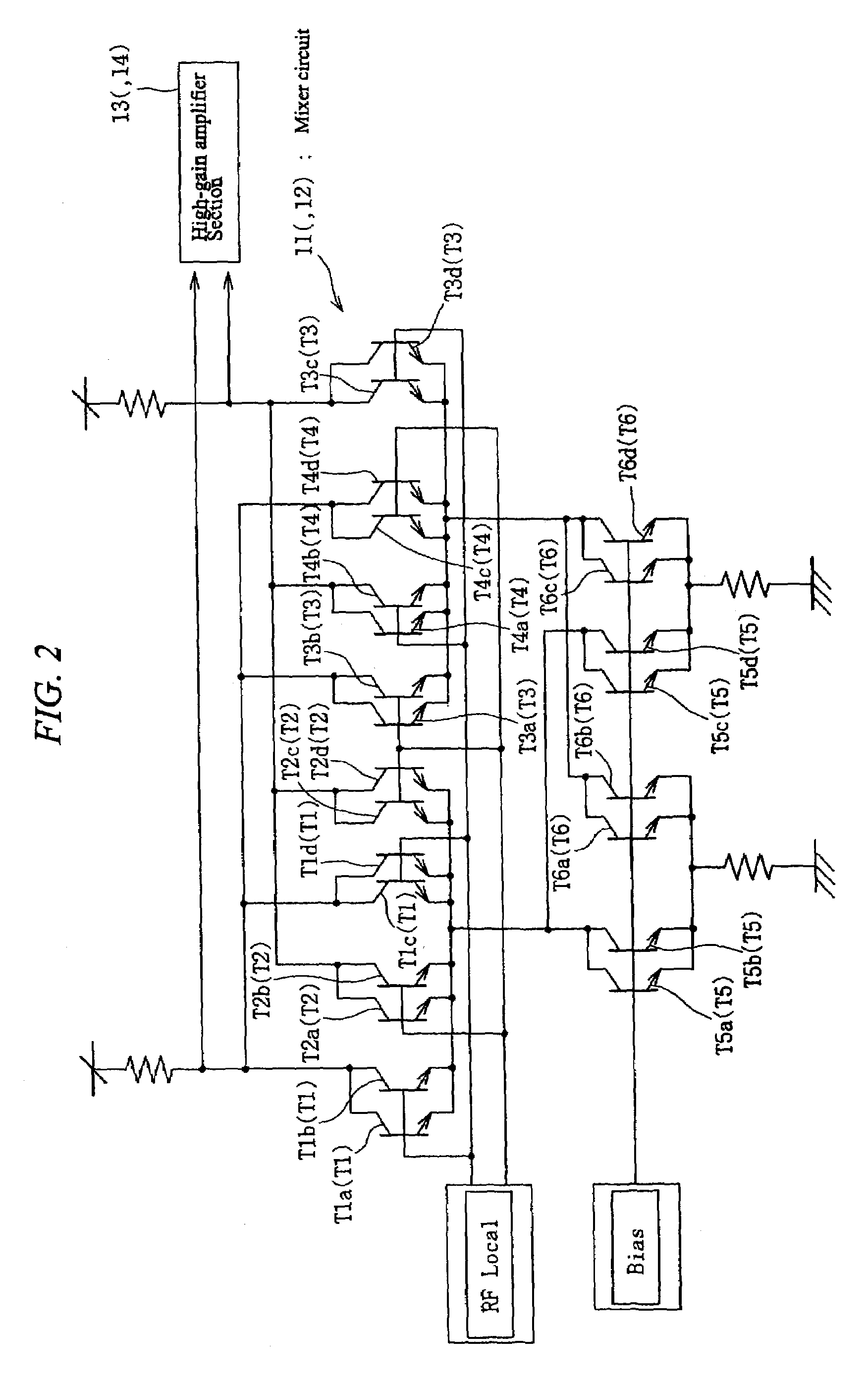
[0031]FIG. 1 is a block diagram of a mobile communication system according to an embodiment of the present invention; FIG. 2 is an equivalent circuit diagram of a mixer section provided in the mobile communication system in FIG. 1; FIG. 3 is an image layout diagram of upper-stage transistors, each of which constitutes a gilbert bell circuit in the mixer section in FIG. 2; FIG. 4 is an image layout diagram of lower-stage transistors, each of which constitutes a gilbert cell circuit in the mixer section in FIG. 2; FIG. 5 is a chip layout diagram of the upper-stage transistors, each of which constitutes the gilbert cell circuit in FIG. 3; FIG. 6 is a chip layout diagram showing an example of the transistors multiple-laid out in FIG. 3; FIG. 7 is a layout diagram of a semiconductor chip on which the transistors in FIG. 4 are provided; FIG. 8 is an explanatory diagram showing a layou...


PUM


Abstract

The thermal interference due to the self heating of transistors constituting a gilbert cell circuit is reduced, thereby largely improving the receiving sensitivity to signals. A mixer circuit composed of a gilbert cell circuit comprises transistors T1 to T6. Each of the transistors T1 to T4 is con figured so that four transistors may be connected in parallel. In a layout on a semiconductor chip, four transistors T1a to T1d and T2a to T2d respectively constituting the transistors T1 and T2 are respectively separated into two pairs, and the respective two pairs are laid out in a crisscross shape so that they are crossed with each other. Similarly, four transistors T3a to T3d and T4a to T4d respectively constituting the transistors T3 and T4 are respectively separated into two pairs, and the respective two pairs are laid out in a crisscross shape so that they are crossed with each other. Thus, the thermal influence applied on the transistors T1 to T4 is uniformed.

Description

BACKGROUND OF THE INVENTION[0001]The present invention relates to a technique for transmitting / receiving radio signals and particularly to a technique effectively applied to the improvement of receiving sensitivity in a cellular phone and the like which use a direct conversion system.[0002]In recent years, a cellular phone has been in widespread use as a device for mobile communication, and there have been increasing demands for a wide variety of functions in the cellular phone. With an aim to reduce the number of electronic parts and the area of a printed wiring board, some cellular phones employ a direct conversion system in a receiving unit of a semiconductor integrated circuit device for a RF (radio frequency) processing.[0003]In the direct conversion system, small signals with a band of 800 MHz to 2 GHz, received by an antenna, are directly converted into signals with a voice band (of about several tens KHz) by the use of one mixer circuit.SUMMARY OF THE INVENTION[0004]However,...

Claims


Application Information

Patent Timeline
Patent Type & Authority Patents(United States)
IPC IPC(8): H04B1/28H04B1/26H01L27/02H03D7/14H03D9/00H04B1/40
CPCH01L27/0207H03D7/1433H03D2200/0047H03D2200/0025H04B1/40
Inventor ONO, IKUYATAGAWA, KAZUHIROTAKAHASHI, SATORU
Owner HITACHI LTD
Why Eureka
Try Eureka