Method of fabricating top gate type thin film transistor having low temperature polysilicon

a polysilicon and top gate technology, applied in the field of thin films, can solve the problems of reducing reliability, reducing electrical characteristics when used in switching devices, and film of amorphous silicon, and achieve the effect of improving the reliability of the silicon oxide layer and improving the silicon oxide layer

Inactive Publication Date: 2006-05-30
LG DISPLAY CO LTD
View PDF43 Cites 31 Cited by
  • Summary
  • Abstract
  • Description
  • Claims
  • Application Information

AI Technical Summary

Benefits of technology

[0019]An advantage of the present invention is to provide a method for fabricating a polysilicon thin film transistor, which has an improved silicon oxide layer.
[0020]Another advantage of the present invention is to provide a method of fabricating a polysilicon thin film transistor, which increases the reliability of the silicon oxide layer.
[0021]Additional features and advantages of the invention will be set forth in the description which follows and in part will be apparent from the description, or may be learned by practice of the invention. The objectives and other advantages of the invention will be realized and attained by the structure particularly pointed out in the written description and claims hereof as well as the appended drawings.
[0022]To achieve these and other advantages and in accordance with the purpose of the present invention, as embodied and broadly described, the present invention provides a method of forming a polysilicon thin film transistor that includes depositing an amorphous silicon layer over a substrate, crystallizing the amorphous silicon layer into a polycrystalline silicon layer, patterning the polycrystalline silicon layer to form a polysilicon active layer for a thin film transistor, depositing silicon oxide over the polysilicon active layer to form a gate insulation layer under a vacuum condition, applying heat to anneal the gate insulation layer under a vacuum condition and forming a gate electrode on the annealed gate insulation layer.
[0023]In another aspect, a method of forming a polysilicon thin film transistor includes forming a buffer layer over a substrate, depositing an amorphous silicon layer over the buffer layer, crystallizing the amorphous silicon layer into a polycrystalline silicon layer, patterning the polycrystalline silicon layer to form a polysilicon active layer, depositing silicon oxide over the polysilicon active layer to form a gate insulation layer under a vacuum condition, applying heat to anneal the gate insulation layer under a vacuum condition, forming a gate electrode on the annealed gate insulation layer, applying dopants to the polysilicon active layer to form source and drain regions, forming an interlayer insulator to cover the gate electrode, the gate insulation layer and the source and drain regions, forming source and drain contact holes in the interlayer insulator to expose portions of the source region and the drain region, respectively, and forming source and drain electrodes.
[0024]It is to be understood that both the foregoing general description and the following detailed description are exemplary and explanatory, and are intended to provide further explanation of the invention as claimed.

Problems solved by technology

However, a thin film of amorphous silicon has some disadvantages, such as decreased reliability, decreased electrical characteristics when used in a switching device, and is difficult to redundantly form in each pixel of a very large area liquid crystal display panel.
At this time, however, there are some disadvantages, i.e., the step of the gate electrode causes the nonuniformity of the polysilicon.
Therefore, the bottom gate type thin film transistor having such polysilicon represents bad electrical characteristics so that the polysilicon layer is hardly used for the bottom gate type thin film transistor.
However, the method of forming the low temperature polysilicon thin film transistor includes some disadvantages.
Furthermore, the operating characteristics of the LTPS-TFT may degrade due to the fact that the silicon oxide gate insulation layer has low resistance against F-N stress (Fowler-Nordheim stress).

Method used


Image

  • Method of fabricating top gate type thin film transistor having low temperature polysilicon
  • Method of fabricating top gate type thin film transistor having low temperature polysilicon
  • Method of fabricating top gate type thin film transistor having low temperature polysilicon

Examples


Embodiment Construction

[0032]Reference will now be made in detail to the embodiments of the present invention, examples of which are illustrated in the accompanying drawings. Wherever possible, the similar reference numbers will be used throughout the drawings to refer to the same or like parts.

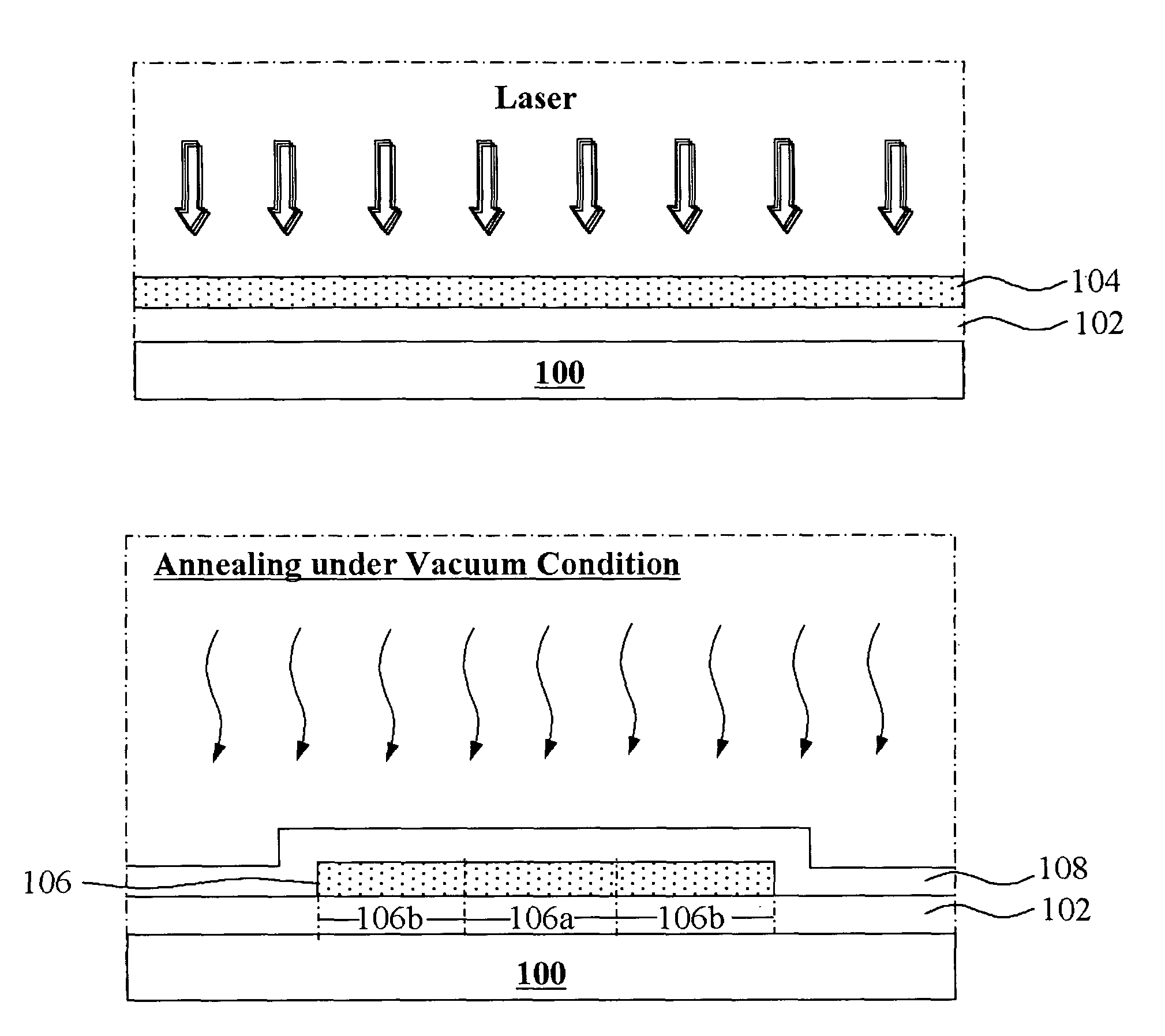
[0033]In exemplary embodiments of the present invention, the reliability of a silicon oxide (SiOx) layer, which is formed by SiH4-based plasma enhanced chemical vapor deposition (PECVD) and implemented in metal-oxide-semiconductor (MOS) capacitors, is improved. Additionally, the characteristics of a low temperature polysilicon thin film transistor (LTPS-TFT) are improved using a more reliable silicon oxide (SiOx) layer. The improvement in the integrity of the silicon oxide (SiOx) layer and device reliabilities using such an improved a silicon oxide (SiOx) layer are achieved by applying an appropriate thermal treatment after silicon oxide deposition. Preferably, after a silicon oxide layer is deposited over a substr...


PUM

PropertyMeasurementUnit
temperatureaaaaaaaaaa
pressureaaaaaaaaaa
flat band voltageaaaaaaaaaa

Abstract

A method of forming a polysilicon thin film transistor that includes depositing an amorphous silicon layer over a substrate, crystallizing the amorphous silicon layer into a polycrystalline silicon layer, patterning the polycrystalline silicon layer to form a polysilicon active layer for a thin film transistor, depositing silicon oxide over the polysilicon active layer to form a gate insulation layer under a vacuum condition, applying heat to anneal the gate insulation layer under a vacuum condition and forming a gate electrode on the annealed gate insulation layer.

Description

[0001]This application claims the benefit of Korean Application No. 2002-53086, filed on Sep. 4, 2002 in Korea, which is hereby incorporated by reference.BACKGROUND OF THE INVENTION[0002]1. Field of the Invention[0003]The present invention relates to a thin film transistor for use in a liquid crystal display device, and more particularly, to a method of fabricating a top gate type thin film transistor (TFT) having low temperature polysilicon.[0004]2. Discussion of the Related Art[0005]In general, silicon is classified into amorphous silicon and crystalline silicon depending on the silicon's crystalline state. It is possible for the amorphous silicon to be formed as a thin film on a glass substrate. Because the glass substrate has a low melting point, the amorphous silicon is deposited at a low temperature on the glass substrate. The amorphous silicon is generally used for a switching device, such as a thin film transistor in pixel of a liquid crystal display panel. However, a thin f...

Claims


Application Information

Patent Timeline
Patent Type & Authority Patents(United States)
IPC IPC(8): H01L21/00H01L21/336H01L29/786
CPCH01L29/66757H01L29/78675H01L29/78609H01L29/786
Inventor LEE, SEOK-WOO
Owner LG DISPLAY CO LTD
Why Eureka
Try Eureka