Antenna structure and installation

a technology of antenna structure and installation, which is applied in the direction of antenna details, antennas, electrical equipment, etc., can solve the problems of increasing the cost of the foregoing typical cost per unit or cost per watt, increasing the cost of conventional power amplification systems of this type generally require considerable additional circuitry, and half of the power consumed in cable loss/heat, etc., to achieve low cost, low power and linear region low cost

Inactive Publication Date: 2006-05-30
COMMSCOPE TECH LLC
View PDF108 Cites 153 Cited by
  • Summary
  • Abstract
  • Description
  • Claims
  • Application Information

AI Technical Summary

Benefits of technology

[0009]In accordance with one aspect of the invention, power amplifier chips of relatively low power and low cost per watt are utilized in a relatively low power and linear region in an infrastructure application. In order to utilize such relatively low power, low cost per watt chips, the present invention proposes use of an antenna array in which one relatively low power amplifier chip is utilized in connection with each antenna element of the array to achieve the desired overall output power of the array.
[0010]Accordingly, a relatively low power amplifier chip typically used for remote and terminal equipment (e.g., handset or user / subscriber equipment) applications may be used for infrastructure (e.g., base station) applications. In accordance with the invention, the need for distortion correction circuitry and other relatively expensive feedback circuits and the like used for linear performance in relatively high power systems is eliminated. The linear performance is achieved by using the relatively low power chips within their linear output range. That is, the invention proposes to avoid overdriving the chips or requiring operation close to saturation level, so as to avoid the requirement for additional expensive and complex circuitry to compensate for reduced linearity. The power amplifier chips used in the present invention in the linear range typically have a low output power of one watt or below. Moreover, the invention proposes installing a power amplifier chip of this type at the feed point of each element of a multi-element antenna array. Thus, the output power of the antenna system as a whole may be multiplied by the number of elements utilized in the array while maintaining linearity.
[0011]Furthermore, the present invention does not require relatively expensive high power combiners, since the signals are combined in free space (at the far field) at the remote or terminal location via electromagnetic waves. Thus, the proposed system uses low power combining avoiding otherwise conventional combining costs. Also, in tower applications, the system of the invention eliminates the power loss problems associated with the relatively long cable which conventionally connects the amplifiers in the base station equipment with the tower-mounted antenna equipment, i.e., by eliminating the usual concerns with power loss in the cable and contributing to a lesser power requirement at the antenna elements. Thus, by placing the amplifiers close to the antenna elements, amplification is accomplished after cable or other transmission line losses usually experienced in such systems. This may further decrease the need for special low loss cables, thus further reducing overall system costs.

Problems solved by technology

The power losses experienced in the cables may necessitate some increase in the power amplification which is typically provided at the ground level infrastructure or base station, thus further increasing expense at the foregoing typical costs per unit or cost per watt.
Moreover, conventional power amplification systems of this type generally require considerable additional circuitry to achieve linearity or linear performance of the communications system.
In this case, half of the power has been consumed in cable loss / heat.
All of this additional circuitry to achieve linearity of the overall system, which is required for relatively high output power systems, results in the aforementioned cost per unit / watt (between $100 and $300).

Method used


Image

  • Antenna structure and installation
  • Antenna structure and installation
  • Antenna structure and installation

Examples


Embodiment Construction

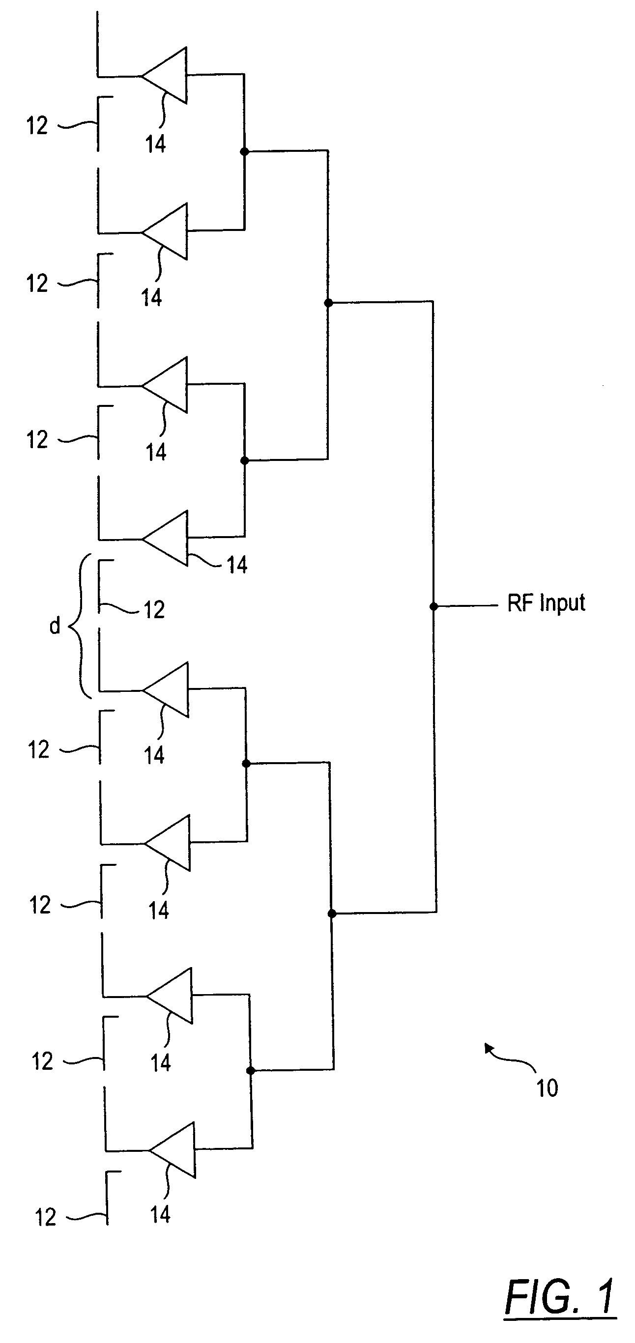
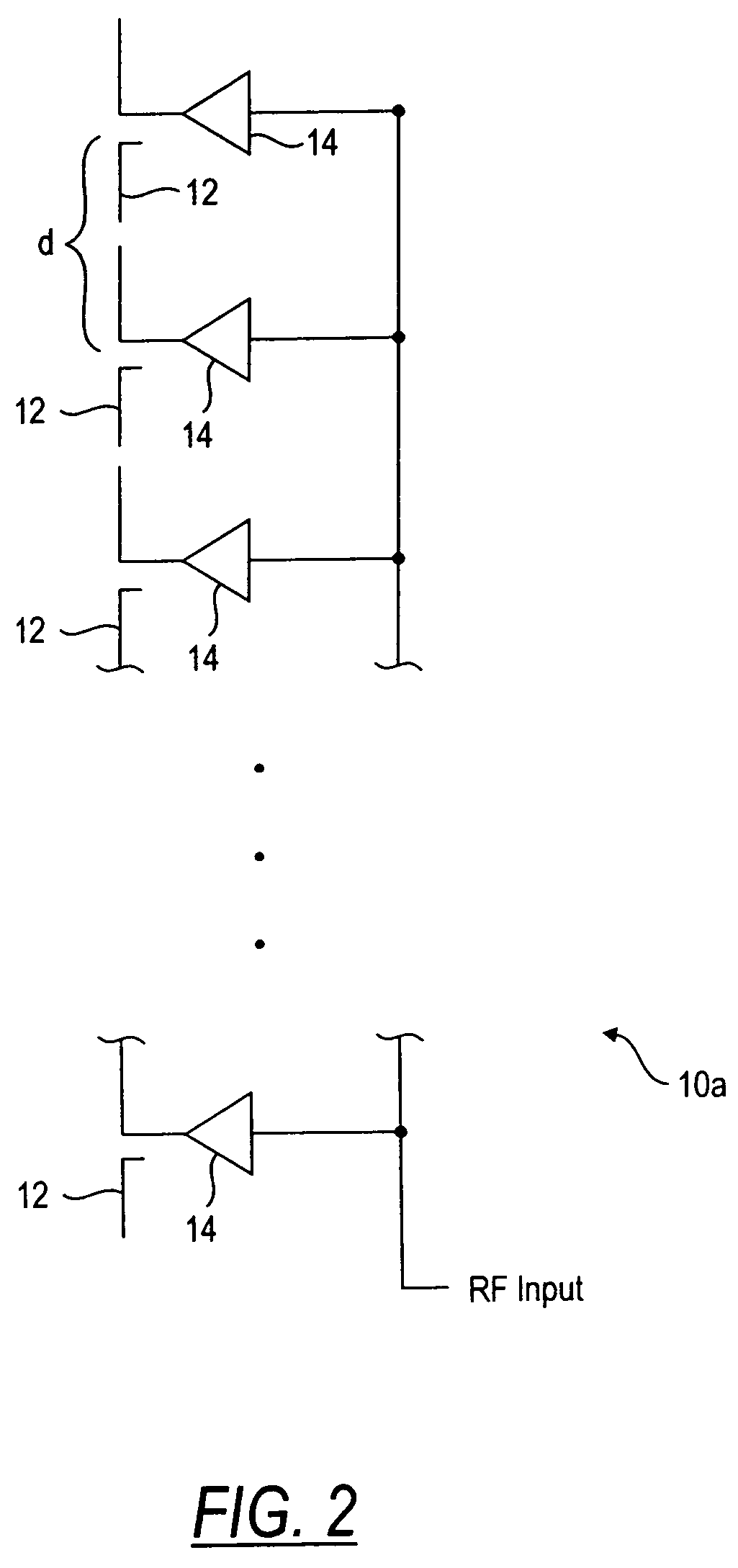
[0020]Referring now to the drawings, and initially to FIGS. 1 and 2, there are shown two examples of a multiple antenna element antenna array 10, 10a in accordance with the invention. The antenna array 10, 10a of FIGS. 1 and 2 differ in the configuration of the feed structure utilized, FIG. 1 illustrating a parallel corporate feed structure and FIG. 2 illustrating a series corporate feed structure. In other respects, the two antenna arrays 10, 10a are substantially identical. Each of the arrays 10, 10a includes a plurality of antenna elements 12, which may comprise monopole, dipole or microstrip / patch antenna elements. Other types of antenna elements may be utilized to form the arrays 10, 10a without departing from the invention.

[0021]In accordance with one aspect of the invention, an amplifier element 14 is operatively coupled to the feed of each antenna element 12 and is mounted in close proximity to the associated antenna element 12. In one embodiment, the amplifier elements 14 a...


PUM


Abstract

An antenna system installation comprising a tower / support structure, and an antenna structure mounted at the top of said tower / support structure, said antenna structure comprises a plurality of antenna elements, a plurality of power amplifiers, each power amplifier being operatively coupled with one of said antenna elements and mounted closely adjacent to the associated antenna element, such that no appreciable power loss occurs between the power amplifier and the associated antenna element, each said power amplifier comprising a relatively low power, relatively low cost per watt linear power amplifier chip, a first RF to fiber transceiver mounted at the top of said tower / support structure and operatively coupled with said antenna structure, and a second RF to fiber transceiver mounted adjacent a base portion of said tower / support structure and coupled with said first RF transceiver by an optical fiber cable.

Description

CROSS-REFERENCE TO RELATED APPLICATION[0001]This application is a continuation of U.S. aplication Ser. No. 09 / 804,178, filed Mar. 12, 2001, and issued as U.S. Pat. No. 6,690,328, which in turn is a continuation-in-part of prior U.S. application Ser. No. 09 / 299,850, filed Apr. 26, 1999, and entitled “Antenna Structure and Installation” and issued as U.S. Pat. No. 6,583,763.BACKGROUND OF THE INVENTION[0002]This invention is directed to a novel antenna structure including an antenna array having a power amplifier chip operatively coupled to, and in close proximity to each antenna element in the antenna array.[0003]In communications equipment such as cellular and personal communications service (PCS), as well as multi-channel multi-point distribution systems (MMDS) and local multi-point distribution systems (LMDS) it has been conventional to receive and retransmit signals from users or subscribers utilizing antennas mounted at the tops of towers or other structures. Other communications...

Claims


Application Information

Patent Timeline
Patent Type & Authority Patents(United States)
IPC IPC(8): H01Q3/22H01Q21/06H01Q1/24H01Q3/28H01Q21/08H01Q23/00H01Q25/04
CPCH01Q1/246H01Q23/00H01Q21/08H01Q3/28
Inventor JUDD, MANO D.
Owner COMMSCOPE TECH LLC
Why Eureka
Try Eureka