Solid-state image pickup device with discharge gate operable in an arbitrary timing

Inactive Publication Date: 2006-05-30
SHARP KK
View PDF14 Cites 36 Cited by
  • Summary
  • Abstract
  • Description
  • Claims
  • Application Information

AI Technical Summary

Benefits of technology

[0023]Accordingly, an object of the present invention is to provide a solid-state image pickup device which can achieve an arbitrary decimation rate without making a complicated wiring structure of vertical transfer electrodes and easily change a frame rate, resolution and the like only by changing drive conditions.
[0028]Consequently, a monitoring mode (decimated reading) can be achieved while vertical transfer electrodes have the same wiring structure as in a still mode (normal reading) without making a complicated vertical transfer electrode wiring structure such as the one in the prior art. In addition, an arbitrary decimation rate can be achieved and a frame rate, resolution and the like can be easily changed only by changing the drive condition of the discharge gate.
[0034]In this embodiment, the discharge gate covers at least part of the vertical transfer section. Therefore, at the time of a transfer, a potential slope is formed in a transfer direction without forming a potential barrier or a potential dip. Therefore, charges in a packet in the vertical transfer section can be completely depleted without causing a defective transfer.
[0036]In this embodiment, a voltage applied to the discharge drain is made variable and a drive timing of a voltage applied to the discharge drain is synchronized with a drive timing of a voltage applied to the discharge gate. Consequently, at the time of a normal charge transfer, leakage of charges to the discharge drain can be prevented by making a potential well of the discharge drain shallow. At the time of a charge discharge operation, charges can be reliably discharged from the vertical transfer section to the discharge drain by making the potential well of the discharge drain deep.
[0038]In this embodiment, a pulse covering the pulse applied to the discharge gate is applied to the discharge drain in a discharge operation mode where the potential in a region under the discharge gate is lowered. Consequently, the charge discharge operation can be reliably performed.
[0040]In this embodiment, one discharge drain is shared by two vertical transfer sections so that the pixel pitch can be reduced and sufficient areas for forming the discharge drain and the discharge gate can be secured even when the pixel size is small.

Problems solved by technology

Therefore, a complicated transfer gate wiring structure is required to achieve a monitoring mode.
Further, to achieve two or more different monitoring modes in one device, the electrode wiring becomes very complicated since a combination of electrode wiring structures for respective decimation rates are required.
The decimation rate of a monitoring mode cannot be changed by changing a drive timing alone.

Method used


Image

  • Solid-state image pickup device with discharge gate operable in an arbitrary timing
  • Solid-state image pickup device with discharge gate operable in an arbitrary timing
  • Solid-state image pickup device with discharge gate operable in an arbitrary timing

Examples


first embodiment

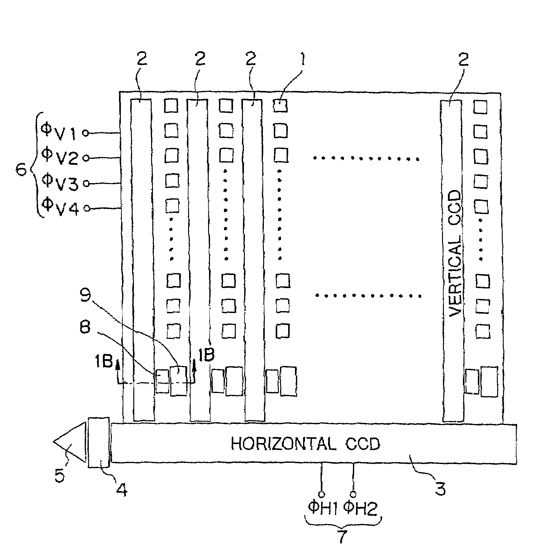
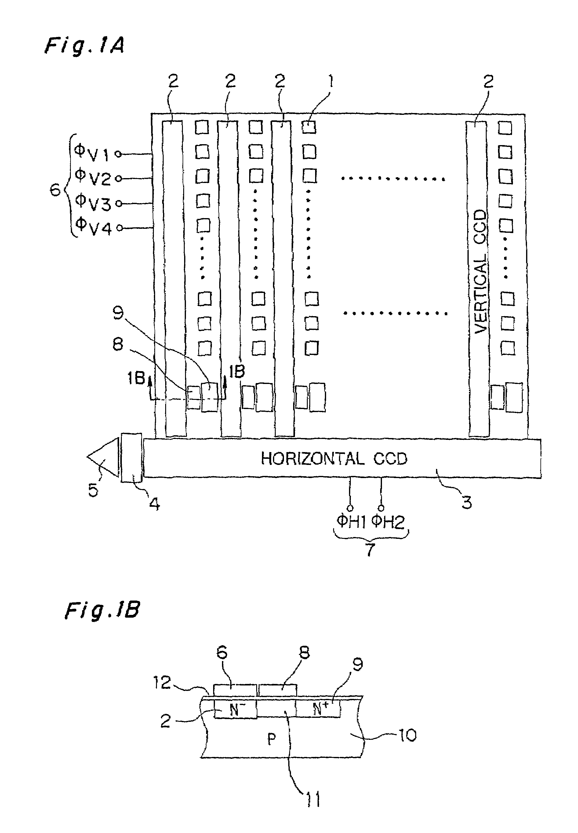
[0062]FIGS. 1A and 1B show a two-dimensional image sensor using CCD (Charge Coupled Device) as an embodiment of the solid-state image pickup device according to the present invention.

[0063]As shown in FIG. 1A, this two-dimensional image sensor is provided with a plurality of vertical CCD 2 arrayed at predetermined intervals and a plurality of light receiving sections 1, 1, 1 . . . , each composed of a photodiode, which are arrayed between these vertical CCD 2. One horizontal CCD 3 is disposed adjacent to one end of the vertical CCD 2, 2, 2 . . . . A charge voltage converting section 4 and an amplifier 5 are successively disposed at one end of the horizontal CCD 3. The vertical CCD 2 has vertical transfer electrodes 6 and the horizontal CCD 3 has horizontal transfer electrodes 7. In this embodiment, the vertical CCD 2, the horizontal CCD 3 and the discharge drain region 9 are n-type semiconductor layers.

[0064]As shown in FIG. 1B, the vertical CCD 2 is formed in a Si substrate 10 made...

second embodiment

[0084]FIG. 5A shows a structure according to a second embodiment of the invention. In the second embodiment, the discharge gate 28 covers part of the vertical CCD 22. In FIG. 5A, reference numeral 22 denotes a vertical CCD, 26 denotes a vertical transfer electrode, 28 denotes a discharge gate, 29 denotes a discharge drain, and 13 denotes a channel stop.

[0085]The second embodiment has a structure for preventing leftover charges, which occurs when the discharge gate 28 and the vertical CCD 22 do not overlap. The discharge gate 28 covers part of the vertical CCD 22.

[0086]FIG. 5B is a cross section view of the potential distribution along 5B-5B in FIG. 5A. When a high voltage is applied to the discharge gate 28, the potential distribution shown with a broken line is obtained and charges are discharged from the vertical CCD 22 towards the discharge drain 29.

[0087]On the other hand, FIGS. 6A–6C are cross sectional views of the potential distribution along 6A—6A in FIG. 5A. These potential...

third embodiment

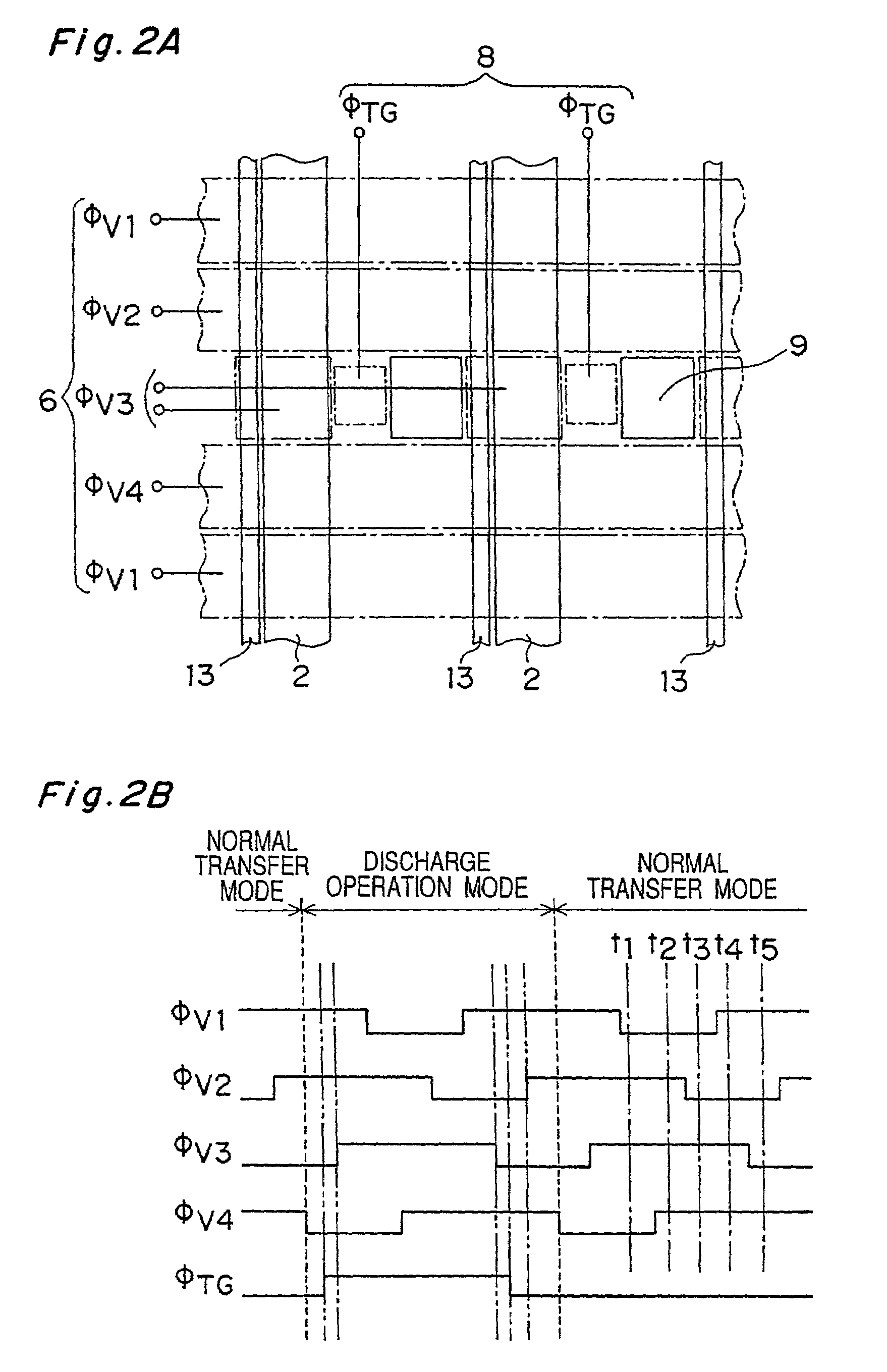
[0092]FIG. 9A shows a layout according to a third embodiment. In the third embodiment, a voltage VD applied to the discharge drain 49 is made variable in the layout according to the second embodiment shown in FIG. 5A.

[0093]FIG. 9B shows waveforms of signals φV1–φV4 to the transfer electrodes 6, a signal φTG to the discharge gate 48 and a voltage VD applied to the discharge drain 49 in the structure shown in FIG. 9A in a normal transfer mode and a discharge operation mode. In the third embodiment, a high voltage VD is applied to the discharge drain in a discharge operation mode during a period including a period when the signal φTG is high as shown in FIG. 9B.

[0094]FIG. 10A is a cross sectional view along 10A—10A in FIG. 9A. FIG. 10B shows a potential distribution corresponding to the cross sectional configuration in FIG. 10A. As shown with a solid line in FIG. 10B, the voltage VD applied to the discharge drain 49 is low and the potential well P1 of the discharge drain 49 is shallow ...


PUM


Abstract

A solid-state image pickup device has a discharge gate and a discharge drain provided adjacent to a connection of a vertical CCD and a horizontal CCD so that charges accumulated for an arbitrary pixel can be completely depleted. Data can be read at an arbitrary decimation rate only by changing a drive condition of the discharge gate. An arbitrary decimation rate can be achieved and a frame rate, resolution or the like can easily changed while vertical transfer electrodes can keep the same wiring structure as in a still mode (normal reading) without making a complicated wiring structure of vertical transfer electrodes such as the prior art. Therefore, this solid-state image pickup device can achieve an arbitrary decimation rate and easily change a frame rate, resolution or the like only by changing drive conditions without making a complicated wiring structure of vertical transfer electrodes.

Description

BACKGROUND OF THE INVENTION[0001]The present invention relates to a solid-state image pickup device, in particular, a solid-state image pickup device for reading decimated signals.[0002]A conventional two-dimensional image sensor will be described below. FIG. 14 shows a solid-state image pickup device using conventional CCD (charge coupled device). In FIG. 14, reference numeral 101 denotes a light receiving section (photodiode), 102 denotes a vertical CCD, 103 denotes a horizontal CCD, 104 denotes an charge voltage converting section, 105 denotes an amplifier, 106 denotes a vertical transfer electrode, and 107 denotes a horizontal transfer electrode.[0003]A two-dimensional image sensor has a higher-density pixels. Particularly, a digital still camera having more than 2 million pixels is becoming a mainstream.[0004]In an image pickup device represented by a high-pixel digital still camera, in general, operation is performed by switching between a drive method where all pixel data is ...

Claims


Application Information

Patent Timeline
IPC IPC(8): H04N3/14H04N5/335H01L27/14H01L27/148H04N5/345H04N5/369H04N5/372
CPCH04N3/1562H01L27/14843H04N25/445H04N25/73H01L27/14
Inventor KONISHI, TOMOHIRO
Owner SHARP KK
Why Eureka
Try Eureka