Substrate based unmolded package including lead frame structure and semiconductor die

a technology of semiconductor die and substrate, which is applied in the direction of semiconductor/solid-state device details, electrical equipment, semiconductor devices, etc., can solve the problems of ceramic materials, relatively thick semiconductor die packages, and relatively high cost of ceramic substrates

Inactive Publication Date: 2006-06-13
SEMICON COMPONENTS IND LLC
View PDF21 Cites 94 Cited by
  • Summary
  • Abstract
  • Description
  • Claims
  • Application Information

AI Technical Summary

Benefits of technology

[0052]Embodiments of the invention have a number of other advantages. First, as noted above, in embodiments of the invention, a lead frame structure is used in a substrate. Lead frame structures are inexpensive and are easy to fabricate. Thus, a substrate according to embodiments of the invention can be made quite inexpensively. For example, the cost of a substrate made according to embodiments of the invention can be reduced by about 70% or more as compared to a ceramic metallized substrate. Second, the substrates according to embodiments of the invention have high contrast between the molding material and the exposed areas of the lead frame structure. As explained in further detail above, this results in fewer defects. Third, embodiments of the invention can be made thinner than conventional semiconductor die packages and substrates. The package size of embodiments of the invention can be reduced by at least 20% over current state of the art packages. For example, the thickness of a semiconductor die package according to an embodiment of the invention can be on the order of about 0.5 mm (or less). Fourth, in embodiments of the invention, the molding process is form factor independent since it is used to construct substrates, and need not be used to completely encapsulate the semiconductor die. Fifth, the substrates and packages of embodiments of the invention can be mounted using well known “flip-chip” techniques. Sixth, in embodiments of the invention, it is possible to etch fine geometries in a lead frame structure so that the package leads and the die attach surface can be customized according to needs. Seventh, the substrates according to embodiments of the invention are mechanically quite rigid, yet flexible enough to be handled in highly automated equipment.

Problems solved by technology

For example, semiconductor die packages that use ceramic substrates are relatively expensive to make.
Compared to many polymeric materials, ceramic materials are expensive.
In addition, both types of semiconductor die packages mentioned above are relatively thick.

Method used


Image

  • Substrate based unmolded package including lead frame structure and semiconductor die
  • Substrate based unmolded package including lead frame structure and semiconductor die
  • Substrate based unmolded package including lead frame structure and semiconductor die

Examples


Embodiment Construction

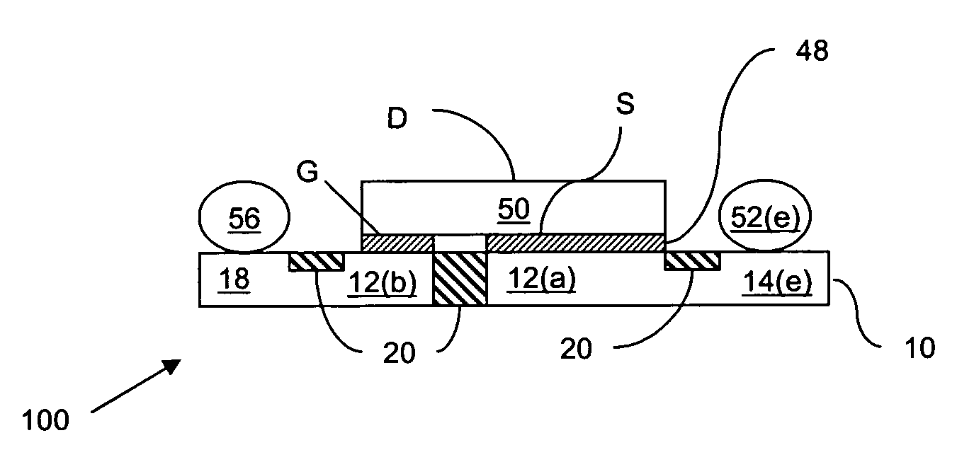
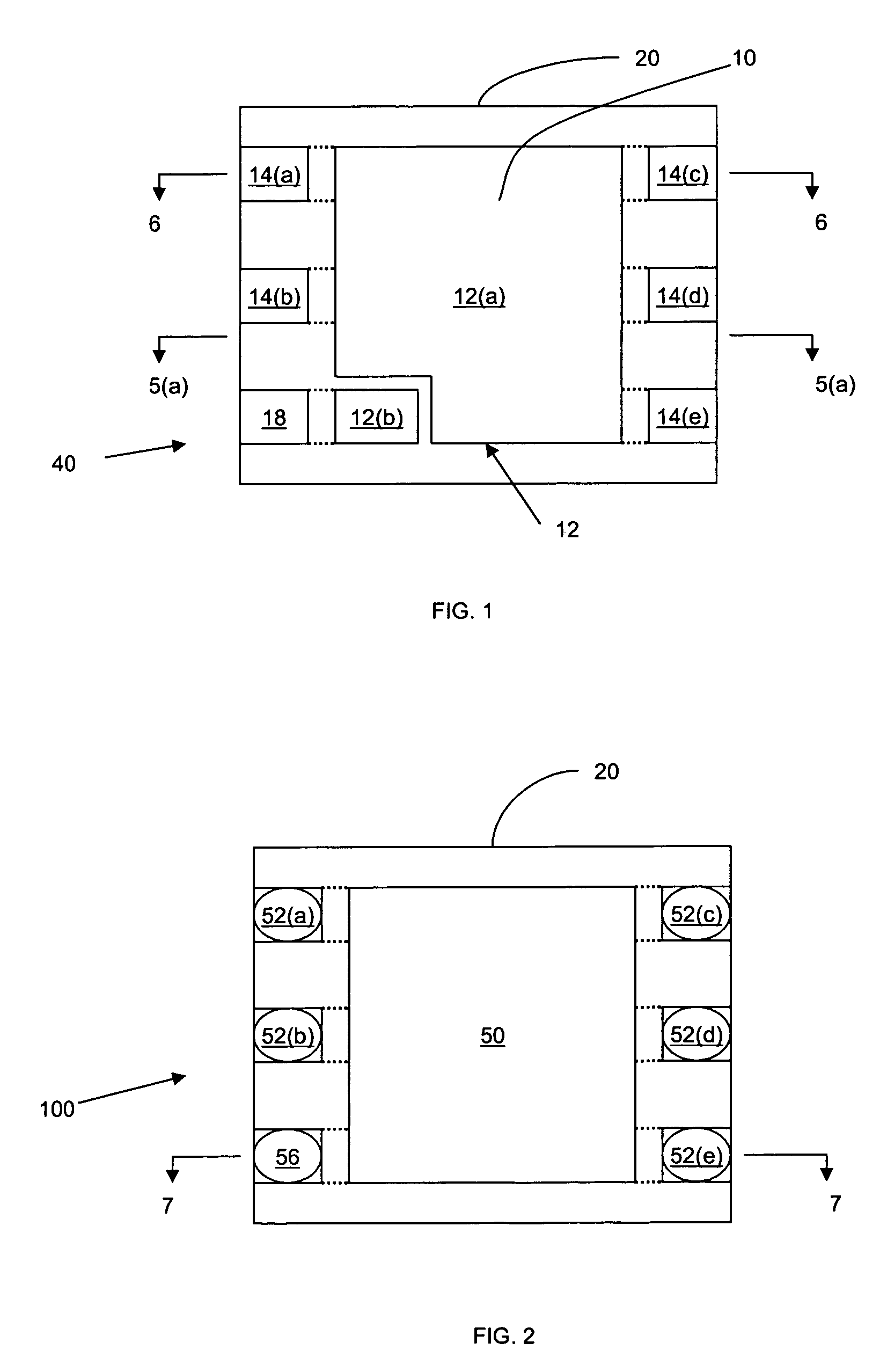
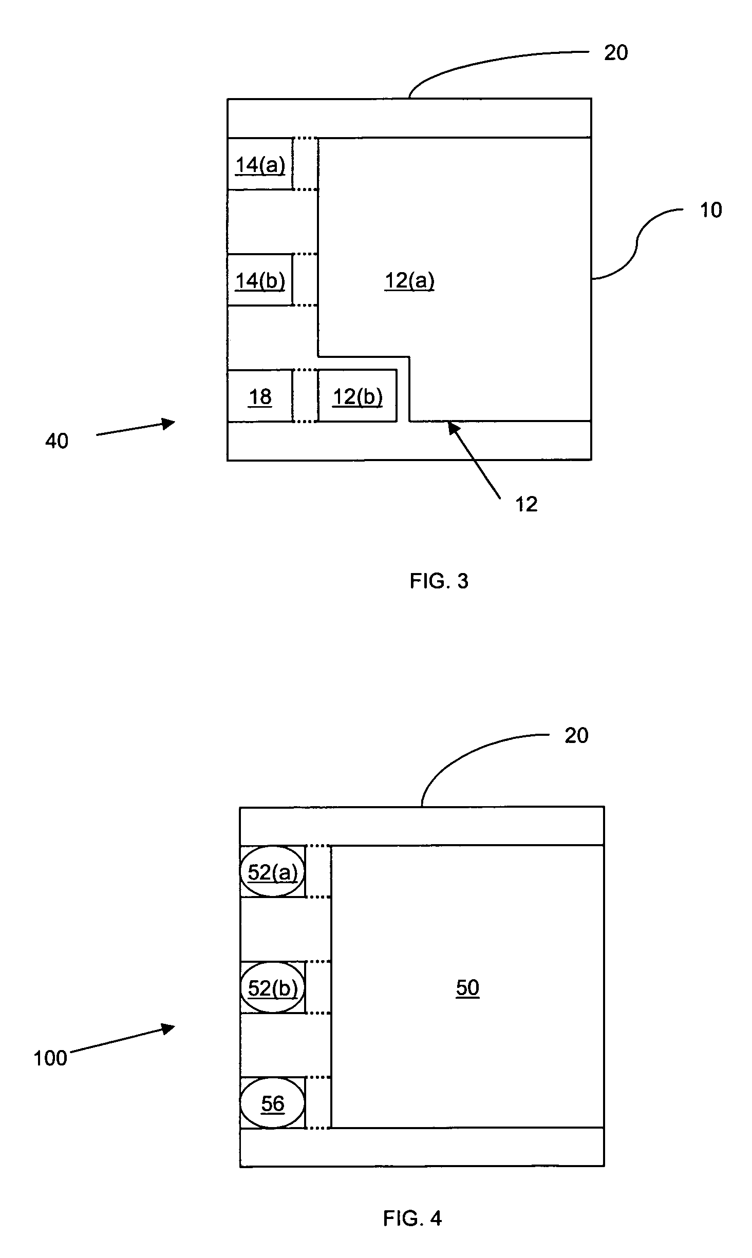
[0021]FIG. 1 shows a substrate 40 according to an embodiment of the invention. The substrate 40 can support a semiconductor die (not shown) in a semiconductor die package.

[0022]The substrate 40 includes a lead frame structure 10 and a molding material 20. The term “lead frame structure” can refer to a structure that is derived from a lead frame. Lead frames can be formed by, for example, a stamping process (known in the art). Lead frames can also be formed by etching a continuous conductive sheet to form a predetermined pattern. However, if stamping is used, the lead frame may originally be one of many lead frames in an array of lead frames that are connected together by tie-bars. During the process of making a semiconductor die package, the lead frame array may be cut to separate the lead frame from other lead frames. As a result of this cutting, portions of a lead frame structure in a final semiconductor die package such as a source lead and a gate lead may be electrically and mec...


PUM


Abstract

A semiconductor die package is disclosed. In one embodiment, the semiconductor die package has a substrate. It includes (i) a lead frame structure including a die attach region with a die attach surface and a lead having a lead surface, and (ii) a molding material. The die attach surface and the lead surface are exposed through the molding material. A semiconductor die is on the die attach region, and the semiconductor die is electrically coupled to the lead.

Description

BACKGROUND OF THE INVENTION[0001]Some conventional semiconductor die packages use ceramic substrates. In one example, a ceramic substrate is metallized and has conductive lines and lands. A semiconductor die is mounted on the ceramic substrate to form a semiconductor die package. This semiconductor die package is then mounted on a circuit board.[0002]Other conventional semiconductor packages use lead frames. In one example, a semiconductor die is mounted to a lead frame with leads. Wires couple the semiconductor die to the leads. The wires, the semiconductor die and then the most of the lead frame (except for the leads that extend outward) are then encapsulated in a molding compound. The molding compound is then shaped. The formed semiconductor die package can then be mounted onto a circuit board.[0003]While such semiconductor packages are useful, improvements could be made. For example, semiconductor die packages that use ceramic substrates are relatively expensive to make. Compare...

Claims


Application Information

Patent Timeline
Patent Type & Authority Patents(United States)
IPC IPC(8): H01L23/495H01L23/12H01L23/498
CPCH01L23/49562H01L24/97H01L23/49861H01L2924/12041H01L2224/48091H01L2924/01004H01L2924/01013H01L2924/01027H01L2924/01029H01L2924/01033H01L2924/01046H01L2924/01047H01L2924/01078H01L2924/01079H01L2924/01082H01L2924/13091H01L2924/19043H01L2924/1306H01L2924/01015H01L24/48H01L2924/01005H01L2924/01006H01L2924/01024H01L2924/014H01L2224/45147H01L2924/00014H01L2924/00H01L2924/15787H01L2924/181H01L2924/12042H01L24/45H01L2224/73265H01L2924/00011H01L2224/45099H01L2924/00012H01L23/495H01L23/12H01L23/28
Inventor JOSHI, RAJEEV
Owner SEMICON COMPONENTS IND LLC
Why Eureka
Try Eureka