Semiconductor built-in millimeter-wave band module

Inactive Publication Date: 2006-06-13
PANASONIC CORP
View PDF23 Cites 33 Cited by
  • Summary
  • Abstract
  • Description
  • Claims
  • Application Information

AI Technical Summary

Benefits of technology

[0008]Therefore, in order to cope with the above-stated conventional problems, it is an object of the present invention to provide a semiconductor built-in millimeter-wave band module by which heat generated from a semiconduct

Problems solved by technology

However, the conventional configuration in which a surface of a material with a high thermal conductivity contacts with a surface of semiconductor device has a problem in that when the semiconductor device is packaged on a wiring board in a face-up manner, an active surface of the semiconductor device contacts with the material with a high thermal conductivity and is covered with the same, which increases an effective dielectric constant at the active surface as compared with the case of contact

Method used


Image

  • Semiconductor built-in millimeter-wave band module
  • Semiconductor built-in millimeter-wave band module
  • Semiconductor built-in millimeter-wave band module

Examples


embodiment 1

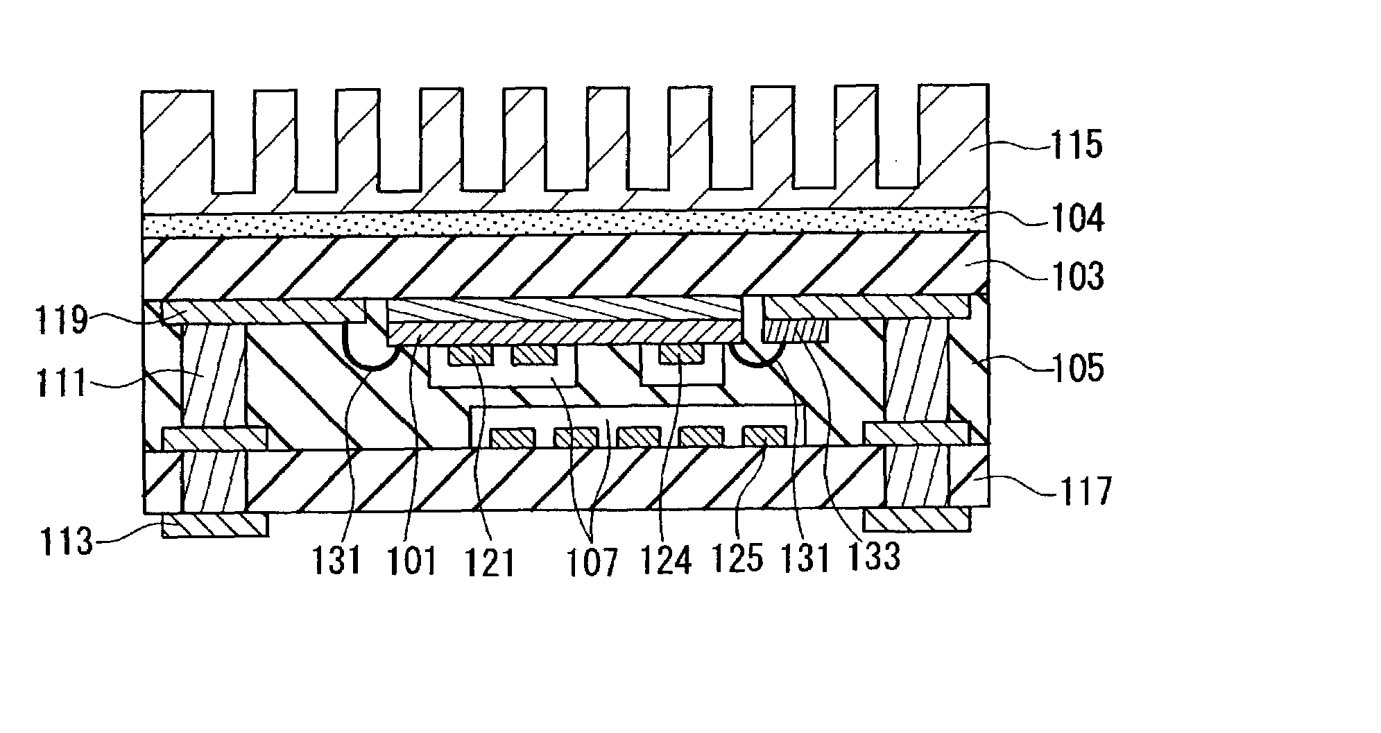
[0052]FIG. 1 is a cross-sectional view schematically showing a configuration of a semiconductor built-in millimeter-wave band module according to Embodiment 1 of the present invention.

[0053]The semiconductor built-in millimeter-wave band module according to this embodiment will be described below, with reference to FIG. 1. In FIG. 1, a semiconductor device 101 is packaged on a high thermal conductivity substrate 103 in a face-up manner and is connected electrically with a wiring pattern 119 formed on the high thermal conductivity substrate 103 and a bypass capacitor 133 mounted on the wiring pattern 119 by means of wire bonding via a wire 131.

[0054]The semiconductor device 101 operates at a millimeter-wave band, and the millimeter-wave band generally refers to 30 GHz or higher, for example, 32 GHz, 60 GHz and 72 GHz, and includes 26 GHz as a special one.

[0055]On the semiconductor device 101, an active element 124 and a passive circuit element 121 (hereinafter referred to as “distrib...

embodiment 2

[0086]FIG. 3 is a cross-sectional view schematically showing a configuration of a semiconductor built-in millimeter-wave band module according to Embodiment 2 of the present invention.

[0087]The following describes the semiconductor built-in millimeter-wave band module of this embodiment, with reference to FIG. 3. In FIG. 3, a semiconductor device 101 is packaged on a high thermal conductivity substrate 103 in a face-up manner and is connected electrically with a wiring pattern 119 formed on the high thermal conductivity substrate 103 and a bypass capacitor 133 mounted on the wiring pattern 119 by means of wire bonding via a wire 131.

[0088]A void 107 is formed at regions of an insulating substrate 105 made of a mixture containing an inorganic filler and a thermosetting resin in the vicinity of a distributed constant circuit element 121 and an active element 124 formed on the semiconductor device 101. On both sides of the insulating substrate 105, the high thermal conductivity substra...

embodiment 3

[0092]FIG. 4 is a cross-sectional view schematically showing a configuration of a semiconductor built-in millimeter-wave band module according to Embodiment 3 of the present invention.

[0093]The following describes the semiconductor built-in millimeter-wave band module of this embodiment, with reference to FIG. 4. In FIG. 4, a semiconductor device 101 is packaged on a high thermal conductivity substrate 103 in a face-up manner and is connected electrically with a wiring pattern 119 formed on the high thermal conductivity substrate 103 and a bypass capacitor 133 mounted on the wiring pattern 119 by means of wire bonding via a wire 131.

[0094]On both sides of an insulating substrate 105, a first and a second high thermal conductivity substrate 103 and 103a are provided, where a wiring pattern 119 provided on the first high thermal conductivity substrate 103 is connected electrically with an external electrode 113 through a via conductor 111 and a via conductor provided in the lower high...


PUM


Abstract

A semiconductor built-in millimeter-wave band module includes: an insulating substrate made of a mixture containing an inorganic filler and a thermosetting resin; a high thermal conductivity substrate made of a dielectric material having thermal conductivity higher than the insulating substrate and laminated on one surface of the insulating substrate; a plurality of wiring patterns formed on the high thermal conductivity substrate and the insulating substrate; a semiconductor device operating at millimeter-wave band, which is arranged inside of the insulating substrate, is packaged on the high thermal conductivity substrate in a face-up manner, and is connected electrically with the wiring patterns; and a distributed constant circuit element and an active element provided on the semiconductor device. In this module, a void is provided inside of the insulating substrate and in the vicinity of a surface of the distributed constant circuit element and the active element. With this configuration, heat from the semiconductor device operating at a millimeter-wave band can be dissipated effectively and the semiconductor and other circuit components can be packaged with high density.

Description

BACKGROUND OF THE INVENTION[0001]1. Field of the Invention[0002]The present invention relates to a semiconductor built-in millimeter-wave band module, and more particularly relates to a semiconductor built-in module in which a semiconductor device operating at a micrometer-wave band or a millimeter-wave band (hereinafter referred to as “semiconductor device operating at a millimeter-wave band”) is arranged inside of an electrical insulating substrate.[0003]2. Related Background Art[0004]In recent years, with a demand for miniaturized electronic equipment having higher performance, circuit components with ever higher density and higher functionality have been demanded. To this end, a circuit board commensurate with the circuit components with higher density and higher functionality has been requested. Especially, as a method for packaging circuit components including a semiconductor device densely, a circuit component built-in module capable of including a semiconductor device therei...

Claims


Application Information

Patent Timeline
IPC IPC(8): H01L23/10H01L23/34H01L21/48H01L21/56H01L23/12H01L23/552H01L23/66H01L25/00H05K1/18
CPCH01L21/481H01L21/56H01L23/552H01L23/66H01L25/162H01L2924/1305H01L2224/45144H01L2924/01322H01L2924/01019H01L24/49H01L2224/48091H01L2224/49171H01L2224/49175H01L2224/73265H01L2924/01046H01L2924/01079H01L2924/14H01L2924/1423H01L2924/1532H01L2924/19041H01L2924/30107H01L2924/3011H01L2924/3025H01L24/48H01L2924/00014H01L2924/00H01L24/45H01L2224/45015H01L2924/12042H01L2924/20752
Inventor IWAKI, HIDEKITAGUCHI, YUTAKAOGURA, TETSUYOSISUGAYA, YASUHIROASAHI, TOSHIYUKINISHIYAMA, TOUSAKUIDOGAWA, YOSHINOBU
Owner PANASONIC CORP
Why Eureka
Try Eureka