Laminated structure and method of manufacturing the same

a technology of laminated structure and manufacturing method, which is applied in the direction of piezoelectric/electrostrictive transducers, mechanical vibration separation, generators/motors, etc., can solve the problems of reducing the detection sensitivity of ultrasonic waves, reducing the performance of piezoelectric actuators, and reducing the electric impedance of elements, so as to relieve the damage of the piezoelectric material layer attributed to the concentration of stress on the insulating region

Inactive Publication Date: 2006-06-13
FUJIFILM HLDG CORP +1
View PDF8 Cites 136 Cited by
  • Summary
  • Abstract
  • Description
  • Claims
  • Application Information

AI Technical Summary

Benefits of technology

[0009]The present invention has been made in view of such problems. An object of the present invention is to provide a laminated structure in which insulating layers are less liable to damage due to stress, and in which interconnections can be easily formed for electrodes.
[0015]According to the present invention, the areas of the insulating regions which are provided in the electrode layers can be made small, so that the damage of the piezoelectric material layer attributed to the concentration of stress on the insulating region can be relieved. Moreover, the electrode layers can be connected by forming the through-holes from the top surface of the laminated piece in which the piezoelectric material layers and the electrode layers are stacked, and then filling up the through-holes with the metal material, so that interconnections can be easily formed even in laminated structures which are arrayed in two dimensions.

Problems solved by technology

In the microfabrication of an element which has opposing electrodes, decrease in the area of the element lowers the capacitance between the electrodes, so that the problem of rise in the electric impedance of the element occurs.
When the electric impedance rises in, for example, a piezoelectric actuator, the impedance matching between the piezoelectric actuator and a signal circuit for driving this piezoelectric actuator cannot be established, and it becomes difficult to feed power to the piezoelectric actuator so that the performance of the piezoelectric actuator degrades.
Further, in an ultrasonic transducer employing a piezoelectric element, the detection sensitivity for an ultrasonic wave degrades.
This results in the problem that the part 106 undergoes stress concentration and is liable to damage.
With such a method, however, it is complicated to form the interconnections for a large number of arrayed laminated structures, respectively.
Especially in the case where laminated structures are arrayed in two dimensions, it is difficult to form the interconnections.

Method used


Image

  • Laminated structure and method of manufacturing the same
  • Laminated structure and method of manufacturing the same
  • Laminated structure and method of manufacturing the same

Examples


first embodiment

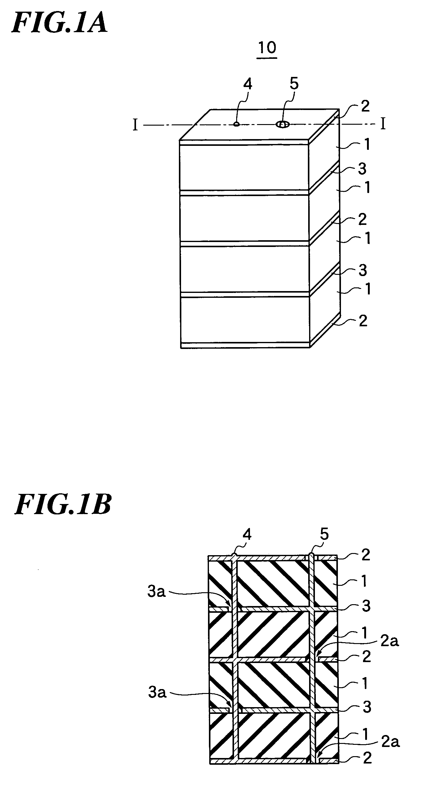
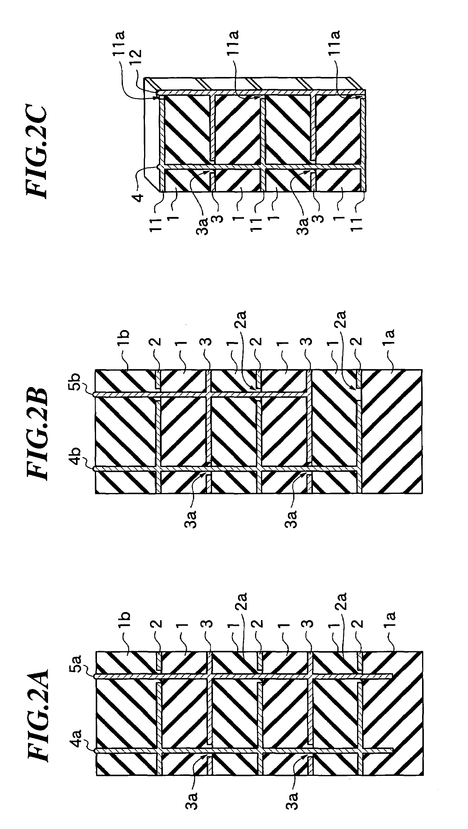
[0031]FIG. 1A is a schematic view showing the construction of a laminated structure according to the present invention, while FIG. 1B is a sectional view taken along I—I in FIG. 1A. As shown in FIG. 1A, the laminated structure 10 is, for example, a minute pillar-like structure having a bottom surface, which has a side of about 0.3–1.0 mm, and a height of about 1.0 mm. This laminated structure 10 includes a plurality of PZT (Pb (lead) zirconate titanate) layers 1, a plurality of first electrode layers 2, a plurality of second electrode layers 3, and vertical interconnection lines 4 and 5.

[0032]The PZT layers 1 are respectively arranged between the first electrode layers 2 and the second electrode layers 3. A voltage is applied between the first electrode layers 2 and the second electrode layers 3, whereby the PZT layers 1 are expanded or contracted by the piezoelectric effect. Such a laminated structure employing a piezoelectric material such as PZT or the like for insulating layers ...

second embodiment

[0055]Next, a laminated structure according to the present invention will be described. FIG. 7 is a perspective view, partly in section, showing the laminated structure according to this embodiment.

[0056]As shown in FIG. 7, the laminated structure according to this embodiment includes a plurality of laminated structures 10 which are arrayed in two dimensions. The construction of each laminated structure 10 is similar to that of the laminated structure 10 described with reference to FIGS. 1A and 1B in the first embodiment of the present invention. In the second embodiment, the plurality of laminated structures 10 are arrayed at intervals of, for example, about 0.3 mm.

[0057]Here, the shape of each laminated structure 10 is not restricted to a rectangular parallelepiped, but it may be any desired shape such as another square pillar or a cylinder. In a case, for example, where the laminated structure according to this embodiment is employed as an ultrasonic transducer array, the shape o...

third embodiment

[0070]Next, a laminated structure according to the present invention will be described. FIG. 11 is a perspective view, partly in section, showing the laminated structure according to this embodiment.

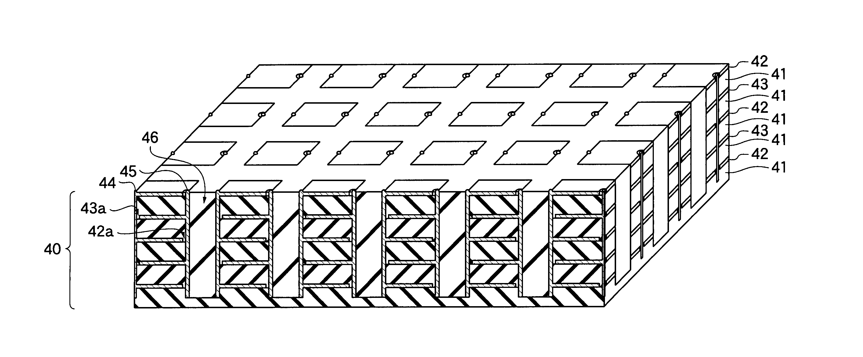
[0071]As shown in FIG. 11, the laminated structure according to this embodiment includes a plurality of laminated structures 40 which are arrayed in two dimensions. An insulating material 46 is packed among the laminated structures 40.

[0072]Each of the laminated structures 40 has the positions of insulating regions and vertical interconnection lines altered from those in the laminated structure 10 shown in FIGS. 1A and 1B, and it includes PZT layers 41, first electrode layers 42, second electrode layers 43, and vertical interconnection lines 44 and 45. In the first electrode layers 42 and the second electrode layers 43, insulating regions 42a and 43a are arranged at end portions within the planes of the respective electrode layers. Besides, the vertical interconnection lines 44 and 45 ar...


PUM


Abstract

A laminated structure in which interconnections can be easily formed for electrodes and in which the damage of an insulating layer attributed to stress is relieved. The laminated structure includes a laminated piece having a first electrode layer provided with a first insulating region, a piezoelectric material layer, and a second electrode layer provided with a second insulating region at a position different from that of the first insulating region, a first interconnection line electrically connected to the first electrode layer while passing through the second insulating region provided in the second electrode layer, and a second interconnection line electrically connected to the second electrode layer while passing through the first insulating region provided in the first electrode layer.

Description

BACKGROUND OF THE INVENTION[0001]1. Field of the Invention[0002]The present invention relates to a laminated structure in which insulator layers and electrode layers are alternately stacked, and a method of manufacturing the laminated structure.[0003]2. Description of a Related Art[0004]Laminated structures in each of which insulator (dielectric) layers and electrode layers are alternately formed, are utilized, not only in laminated capacitors, but also in various other uses such as piezoelectric pumps, piezoelectric actuators and ultrasonic transducers. In recent years, with the developments of devices and equipment concerning MEMS (microelectromechanical systems), elements each having such a laminated structure have been microfabricated still further and packaged more highly.[0005]In the microfabrication of an element which has opposing electrodes, decrease in the area of the element lowers the capacitance between the electrodes, so that the problem of rise in the electric impedan...

Claims


Application Information

Patent Timeline
Patent Type & Authority Patents(United States)
IPC IPC(8): H01L41/083H04R17/00B06B1/06H01L27/20H01L41/047H01L41/09H01L41/187H01L41/22H01L41/23H01L41/293
CPCB06B1/064H01L27/20H01L41/338H01L41/083H01L41/273H01L41/0474H10N39/00H10N30/874H10N30/50H10N30/053H10N30/088
Inventor KUNIYASU, TOSHIAKI
Owner FUJIFILM HLDG CORP
Why Eureka
Try Eureka