Method to detect a defective element

a technology of defective elements and methods, applied in the field of detection methods, can solve the problems of method speed, method is rather slow, method finds quite well not only fabrication errors, but also additional errors that occurred during operation, etc., and achieves the effect of reducing process tim

Active Publication Date: 2006-06-13
MICRONIC LASER SYST AB +1
View PDF32 Cites 56 Cited by
  • Summary
  • Abstract
  • Description
  • Claims
  • Application Information

AI Technical Summary

Benefits of technology

[0007]Accordingly, it is an object of the present invention to provide a method for detecting defective pixels in a spatial light modulator with reduced process time.

Problems solved by technology

Such a method finds quite well not only fabrication errors, but also additional errors that occurred during operation.
On the other hand such method is rather slow, as a high magnification implies that many images have to be taken.

Method used


Image

  • Method to detect a defective element
  • Method to detect a defective element
  • Method to detect a defective element

Examples


Embodiment Construction

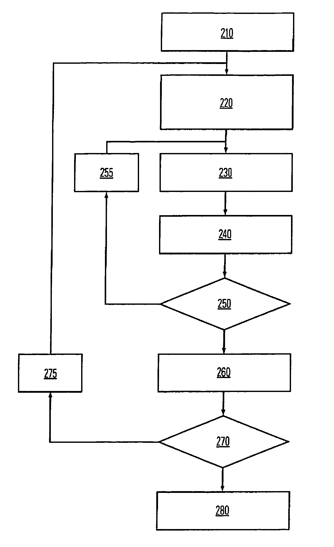
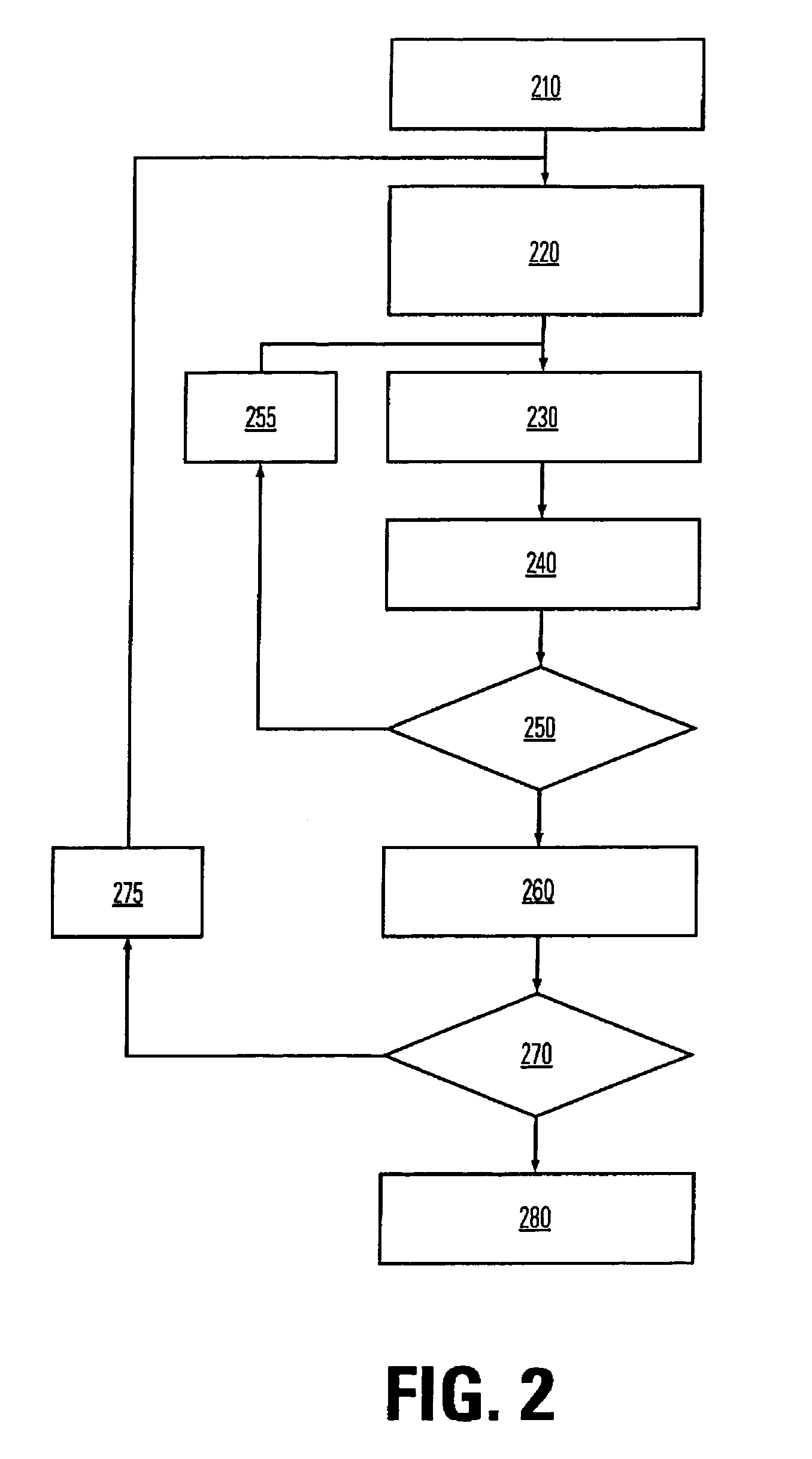
[0062]The following detailed description is made with reference to the Figures. Preferred embodiments are described to illustrate the present invention, not to limit its scope, which is defined by the claims. Those of ordinary skill in the art will recognize a variety of equivalent variations on the description that follows.

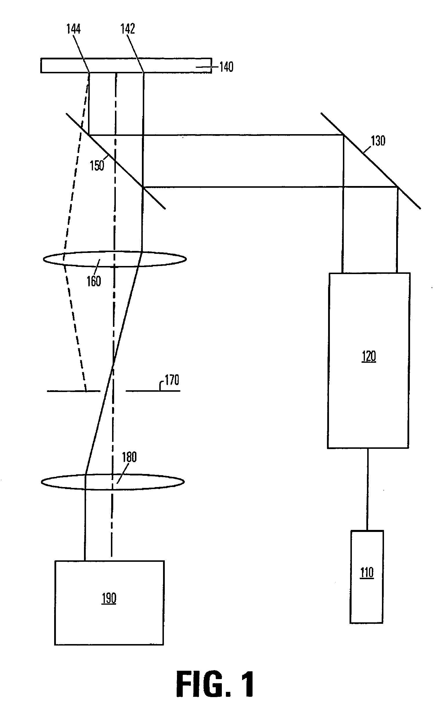
[0063]Further, the preferred embodiments are described with reference to an analogue spatial light modulator (SLM). It will be obvious to one ordinary skill in the art that there may be situations when other SLMs than analogue ones will be equally applicable; for example digital SLMs like a digital micromirror device DMD made by Texas instruments. Additionally, SLMs may comprise reflective or transmissive pixels.

[0064]The invention relates to a method to detect defects in the SLM. Such a method is useful when patterning a workpiece using said spatial light modulator (SLM).

[0065]FIG. 1 illustrates an optical test unit for detecting defective pixels in the spatial ...


PUM

PropertyMeasurementUnit
areaaaaaaaaaaa
electrostatic forceaaaaaaaaaa
applied voltageaaaaaaaaaa

Abstract

The present invention relates to a method to detect at least one defective pixel in a spatial light modulator comprising numerous pixel elements. The spatial light modulator is imaged to a detector. A relayed image of a first chess-board pattern of pixels in said spatial light modulator is detected by said detector. A relayed image of a second chess-board pattern of pixels in said spatial light modulator is detected, which is inverted to the first chessboard pattern, by said detector. The relayed images of said first and second chessboard patterns are analyzed to detect differences between said detected images and theoretical images thereof.

Description

RELATED APPLICATIONS[0001]The present application claims the benefit of and priority to U.S. Provisional Application Ser. No. 60 / 440,145, filed on 15 Jan. 2003, entitled Method to Detect a Defective Element.TECHNICAL FIELD[0002]The present invention relates to a detection method, in particular it relates to a method to detect partially or completely defective pixels in a spatial light modulator.BACKGROUND OF THE INVENTION[0003]Modern UV-lithography is searching for new highly parallel writing concepts. Spatial light modulation (SLM) with optical MEMS devices offers such possibilities. Special emphasis must be put on the ability of SLM devices to handle ultraviolet light (UV), deep ultraviolet light (DUV) and extreme ultraviolet light (EUV).[0004]A SLM chip may comprise a DRAM-like CMOS circuitry with several million individually addressable pixels on top. Said pixels are deflected due to an electrostatic force between a mirror element and an address electrode.[0005]For good performa...

Claims


Application Information

Patent Timeline
Patent Type & Authority Patents(United States)
IPC IPC(8): G01R13/20G01M11/00G02B26/00G03F7/20G09G3/00G09G3/34H04N17/00
CPCG01M11/00G03F7/70291G03F7/70425H04N17/002G09G3/006G03F7/70666G09G3/34G02B26/08
Inventor DURR, PETER
Owner MICRONIC LASER SYST AB
Why Eureka
Try Eureka